Friday, October 31, 2014

Project of UltraSonic Radar Circuit Diagram

- 0 comments
Simple and easy most liked project with many practical applications in security and alarm systems for homes, shops and cars. It consists of a set of ultrasonic receiver and transmitter which operate at the same frequency. When something moves in the area covered by the delicate circuit circuit balance is disturbed and the alarm is activated. The circuit is very sensitive and can be set to zero automatically or to stay on until manually reset after an alarm.

Technical Specifications - Characteristics
Working voltage: 12V DC
Current: 30 mA

How it Works
As it has already been stated the circuit consists of an ultrasonic transmitter and a receiver both of which work at the same frequency. They use ultrasonic piezoelectric transducers as output and input devices respectively and their frequency of operation is determined by the particular devices in use.

The transmitter is built around two NAND gates of the four found in IC3 which are used here wired as inverters and in the particular circuit they form a multivibrator the output of which drives the transducer. The trimmer P2 adjusts the output frequency of the transmitter and for greater efficiency it should be made the same as the frequency of resonance of the transducers in use. The receiver similarly uses a transducer to receive the signals that are reflected back to it the output of which is amplified by the transistor TR3, and IC1 which is a 741 op-amp. The output of IC1 is taken to the non inverting input of IC2 the amplification factor of which is adjusted by means of P1. The circuit is adjusted in such a way as to stay in balance as long the same as the output frequency of the transmitter. If there is some movement in the area covered by the ultrasonic emission the signal

that is reflected back to the receiver becomes distorted and the circuit is thrown out of balance. The output of IC2 changes abruptly and the Schmitt trigger circuit which is built around the remaining two gates in IC3 is triggered. This drives the output transistors TR1,2 which in turn give a signal to the alarm system or if there is a relay connected to the circuit, in series with the collector of TR1, it becomes activated. The circuit works from 9-12 VDC and can be used with batteries or a power supply.

Ultra Sonic Radar Circuit diagram

Project

Construction
First of all let us consider a few basics in building electronic circuits on a printed circuit board. The board is made of a thin insulating material clad with a thin layer of conductive copper that is shaped in such a way as to form the necessary conductors between the various components of the circuit. The use of a properly designed printed circuit board is very desirable as it speeds construction up considerably and reduces the possibility of making errors. Smart Kit boards also come pre-drilled and with the outline of the components and their identification printed on the component side to make construction easier.

To protect the board during storage from oxidation and assure it gets to you in perfect condition the copper is tinned during manufacturing and covered with a special varnish that protects it from getting oxidised and also makes soldering easier. Soldering the components to the board is the only way to build your circuit and from the way you do it depends greatly your success or failure. This work is not very difficult and if you stick to a few rules you should have no problems. The soldering iron that you use must be light and its power should not exceed the 25 Watts. The tip should be fine and must be kept clean at all times.

For this purpose come very handy specially made sponges that are kept wet and from time to time you can wipe the hot tip on them to remove all the residues that tend to accumulate on it. DO NOT file or sandpaper a dirty or worn out tip. If the tip cannot be cleaned, replace it. There are many different types of solder in the market and you should choose a good quality one that contains the necessary flux in its core, to assure a perfect joint every time. DO NOT use soldering flux apart from that which is already included in your solder. Too much flux can cause many problems and is one of the main causes of circuit malfunction. If nevertheless you have to use extra flux, as it is the case when you have to tin copper wires, clean it very thoroughly after you finish your work. In order to solder a component correctly you should do the following:
@Clean the component leads with a small piece of emery paper.

@Bend them at the correct distance from the component’s body and insert the component in its place on the board.

@You may find sometimes a component with heavier gauge leads than usual, that are too thick to enter in the holes of the p.c. board.

@In this case use a mini drill to enlarge the holes slightly. Do not make the holes too large as this is going to make soldering difficult afterwards.

@Take the hot iron and place its tip on the component lead while holding the end of the solder wire at the point where the lead emerges from the board. The iron tip must touch the lead slightly above the p.c. board.

@When the solder starts to melt and flow wait till it covers evenly the area around the hole and the flux boils and gets out from underneath the solder. The whole operation should not take more than 5 seconds. Remove the iron and allow the solder to cool naturally without blowing on it or moving the component. If everything was done properly the surface of the joint must have a bright metallic finish and its edges should be smoothly ended on the component lead and the board track. If the solder looks dull, cracked,or has the shape of a blob then you have made a dry joint and you should remove the solder (with a pump, or a solder wick) and redo it.
@Take care not to overheat the tracks as it is very easy to lift them from the board and break them.

@When you are soldering a sensitive component it is good practice to hold the lead from the component side of the board with a pair of long-nose pliers to divert any heat that could possibly damage the component.

@Make sure that you do not use more solder than it is necessary as you are running the risk of short-circuiting adjacent tracks on the board, especially if they are very close together.

@When you finish your work cut off the excess of the component leads and clean the board thoroughly with a suitable solvent to remove all flux residues that may still remain on it.

@There are quite a few components in the circuit and you should be careful to avoid mistakes that will be difficult to trace and repair afterwards. Solder first the pins and the IC sockets and then following if that is possible the parts list the resistors the trimmers and the capacitors paying particular attention to the correct orientation of the electrolytic.

@Solder then the transistors and the diodes taking care not to overheat them during soldering. The transducers should be positioned in such a way as they do not affect each other directly because this will reduce the efficiency of the circuit. When you finish soldering, check your work to make sure that you have done everything properly, and then insert the IC’s in their sockets paying attention to their correct orientation and handling IC3 with great care as it is of the CMOS type and can be damaged quite easily by static discharges. Do not take it out of its aluminium foil wrapper till it is time to insert it in its socket, ground the board and your body to discharge static electricity and then insert the IC carefully in its socket. In the kit you will find a LED and a resistor of 560 — which will help you to make the necessary adjustments to the circuit. Connect the resistor in series with the LED and then connect them between point 9 of the circuit and the positive supply rail (point 1).

Connect the power supply across points 1 (+) and 2 (-) of the p.c. board and put P1 at roughly its middle position. Turn then P2 slowly till the LED lights when you move your fingers slightly in front of the transducers. If you have a frequency counter then you can make a much more accurate adjustment of the circuit. Connect the frequency counter across the transducer and adjust P2 till the frequency of the oscillator is exactly the same as the resonant frequency of the transducer. Adjust then P1 for maximum sensitivity. Connecting together pins 7 & 8 on the p.c. board will make the circuit to stay triggered till it is manually reset after an alarm. This can be very useful if you want to know that there was an attempt to enter in the place which are protected by the radar.


Adjustments
This kit does not need any adjustments, if you follow the building instructions.

Warning
If they are used as part of a larger assembly and any damage is caused, our company bears no responsibility.
While using electrical parts, handle power supply and equipment with great care, following safety standards as described by international specs and regulations.

If it does not work
Check your work for possible dry joints, bridges across adjacent tracks or soldering flux residues that usually cause problems. Check again all the external connections to and from the circuit to see if there is a mistake there.

See that there are no components missing or inserted in the wrong places.
Make sure that all the polarised components have been soldered the right way round. Make sure that the supply has the correct voltage and is connected the right way round to your circuit. Check your project for faulty or damaged components.

If everything checks and your project still fails to work, please contact your retailer and the Smart Kit Service will repair it for you.

Parts
R1 180 KOhm
R2 12 KOhm
R3, 8 47 KOhm
R4 3,9 KOhm
R5, 6, 16 10 KOhm
R7, 10, 12, 14, 17 100 KΩ
R9, 11 1 MOhm
R13, 15 3,3 KOhm
C1, C6 10uF/16V
C2 47uF/16V
C3 4,7 pF
C4, C7 1 nF
C5 10nF
C8, C11 4,7 uF/16V
C9 22uF/16V
C10 100 nF
C12 2,2 uF/16V
C13 3,3nF
C14 47nF
TR1, 2, 3 BC547 , BC548
P1 10 KOhm trimmer
P2 47 KOhm trimmer
IC1, 2 741 OP-AMP
IC3 4093 C-MOS
R TRANSDUCER 40KHz
T TRANSDUCER 40KHz
D1, 2, 3, 4 1N4148

Author:smartkit,Sourced by http://saaqibs.blogspot.com/
[Continue reading...]

Thursday, October 30, 2014

Lighting Up Model Aircraft Circuit Diagram

- 0 comments
Lighting Up Model Aircraft Circuit diagram :


Lighting Up Model Aircraft Circuit Diagram

All signals are generated by a 4060 14-stage binary counter and some minimal output selection logic. Cycle time is determined by the way the internal oscillator is con-figured (resistor and capacitor on pins 9/10) and can be varied within quite broad limits. High-efficiency LEDs are your first choice for the indicators connected to the Bea-con and Strobe outputs (remember to fit series resistors appropriate to the operating voltage Ub and the current specified for the LED used). 

The sample circuit is for operating voltages between 5 and 12 V. Cur- rent flow through the two BS170 FET devices must not exceed 500 mA.


Author : Werner Ludwig
[Continue reading...]

using L200 Battery Charger Circuit Diagram

- 0 comments
This is a simple circuit using L200 Battery Charger Circuit Diagram. A very simple battery charger circuit having reverse polarity indication is shown here.The circuit is based on IC L200 . L200 is a five pin variable voltage voltage regulator IC. The charging circuit can be fed by the DC voltage from a bridge rectifier or center tapped rectifier.Here the IC L200 keeps the charging voltage constant.The charging current is controlled by the parallel combination of the resistors R2 & R3.The POT P1 can be used to adjust the charging current.

 Battery charger circuit using L200 With Parts list


This circuit is designed to charge a 12 V lead acid battery.The transistor t1,diode D3 and LED are used to make a battery reverse indicator.In case the battery is connected in reverse polarity ,the reverse polarity indicator red LED D5 glows.When the charging process is going on the battery charging indicator green LED D4 glows.

Notes.
The circuit can be assembled on a good quality PCB or common board.
The values of R2 & R3 can be obtained from the equation,
(R2//R3) =( V5-2)/(Io).
Where V5 is  the charging voltage (voltage at pin 5) and Io is the charging current.
The POT R8 can be used for fine adjustments of charging current.
If battery is connected in reverse polarity the RED LED will glow.
When the  charging is going on the GREEN LED will glow.
The rectified input voltage to the charger can be 18V.


Sourced By: Circuitsstream
[Continue reading...]

Wednesday, October 29, 2014

Low Cost Universal Battery Charger Schematic

- 0 comments
This is the circuit diagram of a low cost universal charger for NiCD - NiMH batteries. This circuit is Ideal for car use. It has ability to transform a mains adapter in to a charger . This one can be used to charge cellular phone, toys, portables, video batteries, MP3 players, ... and has selectable charge current. An LED is located in circuit to indicate charging. Can be built on a general purpose PCB or a veroboard. I hope you really like it.

Picture of the circuit:

 a_low_cost_universal_charger 
 A Low Cost Universal Charger Circuit Schematic
Circuit diagram:
a_low_cost_universal_charger_circuit_diagram_for_nicd
A Low Cost Universal Charger Circuit Diagram


Parts:
R1 = 120R-0...5W
R2 = See Diagram
C1 = 220uF-35V
D1 = 1N4007
D2 = 3mm. LED
Q1 = BD135
J1 = DC Input Socket
Specifications:
  • Ideal for in car use.
  • LED charge indication.
  • Selectable charge current.
  • Charges Ni Cd or NiMH batteries.
  • Transforms a mains adapter into a charger.
  • Charge cellular phone, toys, portables, video batteries …
Features:
  • LED function indication.
  • Power supply polarity protected.
  • Supply current: same as charge current.
  • Supply voltage: from 6.5VDC to 21VDC (depending on used battery)
  • Charge current (±20%): 50mA, 100mA, 200mA, 300mA, 400mA. (selectable)
Determining the supply voltage:
This table indicates the minimum and maximum voltages to supply the charger. See supply voltage selection chart below.
Example:
To charge a 6V battery a minimum supply voltage of 12V is needed, the maximum voltage is then 15V.
Voltage selection:

supply_voltages_selection_chart_for_
Voltage Selection Chart For Low Cost Universal Battery Charger

Determining the charge current:
Before building the circuit, you must determinate how much current will be used to charge the battery or battery pack. It is advisable to charge the battery with a current that is 10 times smaller then the battery capacity, and to charge it for about 15 hours. If you double the charge current , then you can charge the battery in half the time. Charge current selection chart is located in diagram.

Example:
A battery pack of 6V / 1000mAh can be charged with 100mA during 15 hours. If you want to charge faster, then a charge current of 200mA can be used for about 7 hours.
Caution:
The higher charge current, the more critical the charge time must be checked. When faster charging is used, it is advisable to discharge the battery completely before charging. Using a charge current of 1/10 of the capacity will expand the lifetime of the battery. The charge time can easily be doubled without damaging the battery.
Note:
  • Mount the transistor together with the heatsink on the PCB, bend the leads as necessary. Take care that the metal back of the transistor touches the heatsink. Check that the leads of the transistor do not touch the heatsink.
[Continue reading...]

Tuesday, October 28, 2014

TDA7383 35W Car Quad Audio Amplifier diagram

- 0 comments
The following a 4 x 35 watts channels/quad audio power amplifier circuit based IC TDA7383. The amplifier circuit is designed specifically suitable for car audio system applications. With a fairly large output power per channel, low distortion and low output noise features. Heatsink should be installed on the power IC to avoid excessive heat. There are very simple and easy to build cos only a few additional components outside the IC power.

Circuit  4 x 35W Car Audio Amplifier TDA7383


IC TDA7383 is a new technology class AB Audio Power Amplifier in Flexiwatt 25 package designed for high end car radio applications. Thanks to the fully complementary PNP/NPN output configuration the TDA7383 allows a rail to rail output voltage swing with no need of bootstrap capacitors. The extremely reduced components count allows very compact sets. The on-board clipping detector simplifies gain compression operations. The fault diagnostics makes it possible to detect mistakes during Car- Radio assembly and wiring in the car.

Absolute Maximum Ratings of IC TDA7383
Operating Supply Voltage : 18 V
DC Supply Voltage : 28 V
Peak Supply Voltage (t = 50ms) : 50 V
Output Peak Current Repetitive (Duty Cycle 10% at f = 10Hz): 4.5 A
Output Peak Current Non Repetitive (t = 100µs) : 5.5 A
Power dissipation, (Tcase = 70°C) : 80 W
Junction Temperature : 150 °C
Storage Temperature : – 55 to 150 °C
[Continue reading...]

Monday, October 27, 2014

Shift registers 74LS164

- 0 comments
This is a TTL shift registers they use voltage source when using the 3V-5V. And it is often used along with the support of the NE555 oscillator in the lab. Image simulation.


How it works: we only need to change in logic value at pin 1 of the  74LS164  is running you will see a change in the value of the led out.

P / S:  Do we only have one class hour his practice should only do this to support you. Wish you have a practice test session to achieve good results.
[Continue reading...]

Know the Line Follower Robot

- 0 comments
Line Follower Robot Glance - Line Follower Robot- a kind of robot which included into the category robotmobile are designed to work in an autonomous and have the ability to detect and move to follow (follows) the existing line on the surface. Control system used is designed to feel that there are pathways of movement and maneuver in order to remain able to follow that line. Robots of this type quite a lot of interest for those who are just learning to robot technology. Even competitions Line Follower Robot, often held regularly at various universities .In industry, robots of this type is often used to to move goods from one place to another. By modifying slightly the sensor line follower robot can then be developed into a Wall Follower Robot, a robot that can move around the wall.


Sensor On Line Follower Robot Sensors, can be analogous to the eye of a robot that serves to read the black line of the track robot. So that the robot is able to know when he will turn right, when he turned left and when he stopped. The sensor used is a light sensor mounted below the front of the robot, so as to find a bright line of a dark background or vice versa. Sensors used are usually photo reflector, R LD (Light Dependent Resistor), Photo Diodes and Photo Transistor - mounted on the front two or more under robotline follower. There also are using the camera as a sensor (or image sensor) to a higher-resolution readout line, making more accurate robot motion.

The working principle of the sensor is simple, when the transmitter (infrared) emitting light onto a white field, the light will be reflected almost entirely by the white areas. In contrast, Itter m ans when emit light to dark or black areas, then the light will be absorbed by the dark areas, so that incoming light kereceiver low. To be able to read by the microcontroller, the sensor voltage should be adjusted to TTL voltage level that is 0-1 volts for logic 0 and 3-5 volts for logic 1. This can be done by installing the operational amplifier is used as a comparator.
[Continue reading...]

Thursday, October 23, 2014

Simple Inverter with Two Transistors

- 0 comments
The series below is a simple inverter circuit that will change the voltage of 12v dc to 220v ac, with use drive transistor 32 as its tip.  Inverter circuit is very simple and easy to assemble and is perfect for just starting to learn to assemble electronic circuits, you can use the transformer 2A to produce about 20 watts output. Do not forget to install coolers in its transistors. good luck.
Simple
[Continue reading...]

ADC 0804 Microcontroler Interface Engineering

- 0 comments
Microcontroller Interface Engineering With ADC 0804
In ADC 0804 interface techniques with microcontrollers are pin-pin control must be controlled if we want to use the ADC with the microcontroller, there is value addition refferensi voltage to be supplied in 0804 ADC interface with a microcontroller, for example, we use the 0804 ADC (8 bit), if we give refferensi voltage 2.55 volts then we will get the increase of 1 bit to change 10 mVolt. Please note that the 0804 ADC pin on the leg that is form Vref Vref / 2, so to get a 10mV resolution is necessary for setting Vref / 2 equal to 1.275 V
The interface circuit microcontroller with ADC 0804


Mechanical interface microcontroller with ADC 0804
The steps in accessing data from the ADC 0804 by the microcontroller sebgai follows;

Enable ADC with signal 0 at the foot of Chip Select.
Give commands from conversion by providing a low pulse to the foot of the ADC Write narrow
Wait for the ADC issued a signal 0 from his leg INT
Give a moment of time delay for data from the ADC is correct
Give the read command by giving the signal 0 at the foot of ADC Read
Give a moment of time delay
Now data from the ADC is ready for use and if the microcontroller.
[Continue reading...]

Saturday, October 18, 2014

MJ2955 78XX Increasing Regulator Current circuit and explanation

- 0 comments

Notes:
Although the 78xx series of voltage regulators are available with different current outputs, you can boost
the available current output with this circuit. A power transistor is used to supply extra current to the load
the regulator, maintaining a constant voltage. Currents up to 650mA will flow through the regulator, above
this value and the power transistor will start to conduct, supplying the extra current to the load. This should
be on an adequate heat sink as it is likely to get rather hot. Suppose you use a 12v regulator, 7812. The
input voltage should be a few volts higher to allow for voltage drops. Assume 20 volts. Lets also assume
that the load will draw 5amps. The power dissipation in the transistor will be Vce * Ic or (20-12)*8=40watt.
It may keep you warm in the Winter, but you will need a large heatsink with good thermal dissipation.
If you want to increase the output current with a negative regulator, such as the 79xx series, then the circuit
is similar, but an NPN type power transistor is used instead.

Source ::
http://www.mitedu.freeserve.co.uk/Circuits/Power/boosti.htm
[Continue reading...]

Friday, October 17, 2014

25L6 Amplifier

- 0 comments
25L6 Amplifier Schematic


25L6 Amplifier
[Continue reading...]

Thursday, October 16, 2014

Simple Power Pulse Using by LM350 and NE555 Circuit Diagram

- 0 comments
This is a Simple Power Pulse Using by LM350 and NE555 Circuit Diagram. This circuit can use to drive lamp,power LED,DC motor etc. Adjust R5 for output amplitude.Adjust R1 for output power .

Power Pulse Circuit Diagram


The LM350 is adjustable 3-terminal positive voltage regulators is capable of supplying in excess of 3A over a 1.2V to 33V output range.This circuit requires 5-15V power supply.
[Continue reading...]

12V to 120V DC DC Converter Circuit

- 0 comments

12V to 120V DC DC Converter Circuit

Here is a simple DC DC converter schematic using a saturation-limited to push-pull converter. DC converter can be used to power the VCR from a car battery and glow plug light aircraft models from a 12V battery starter.

As a final amplifier of the DC DC converter is a pair of transistor MJE2955 and 2SC945 as oscillator to apply sufficient bias to the final amplifier transistors.

The 2SC945 is a bias switch for startup. When applying 12V power, this transistor applies enough bias to the power transistors to get the oscillation started. Soon later, the 100uF capacitor charges up, the transistor goes off, and the power transistors self-bias into cut-off, such that cross-conduction is eliminated. After removing power, the 6k8 resistor discharges the bias timing capacitor, as otherwise the circuit would be unable to restart!

The secondary rectifiers are ultrafast diodes. These are NOT 1N4007! And the 220nF capacitors for the secondary filter are no typos; the diodes deliver almost pure DC, since the oscillation waveform is square, so only some noise filtering is needed. No electrolytics are necessary here.

12V

DC DC Converter

Note the filters at both input and output, using ferrite cores. These are necessary to avoid polluting your environment with RF noise! Using these filters, and joining the input and output negative leads, this converter is very quiet and does not cause any problem in my combined HF, VHF and UHF station.

All ferrite cores (for the transformer and for the noise filters) are manufactured by Amidon Associates, and can be ordered directly from them in small quantities. Look for Amidon on the web. The 77-material core used for the transformer is less than ideal. A square-loop ferrite would work more efficiently! This one gets really warm, operating in saturation mode at 25 kHz. But it has worked well enough for two years now. The filter cores, on the other hand, are well chosen, so try to use the exact ones.

For all windings, the schematic states the number of turns. “7t” means 7 turns. As the transformer is quite small for the involved power, use as thick a wire as you can fit, leaving about half of the space for the 2×7 turns primary winding, and the other half for the secondary, while the feedback winding can be made from very thin wire.

The transistors do not need any heat sinks. They are large enough without, and they need to dissipate little heat!

[Continue reading...]

Wednesday, October 15, 2014

Build a Fly back Transformer Driver Circuit Diagram

- 0 comments
This is an efficient flyback driver for modern cylindrical rectified television flybacks. Many sites doesnt provide circuits driving these transformers, they simply say that they are bad.

I dont agree. In fact I built this circuit. I spent a lot of time for finding resonant frequency (around 15Khz) and duty cycle. These transformers best work at around 90% duty cycle. You may notice corona breakdown at terminals and pfffff sound (as well as the ozone smell) when adjusting the off time trimmer to near 500-300 ohms. Of course it will work for other tipes of flyback as frequency and duty cycle have a large range.

 Flyback Transformer Driver Circuit Diagram


Flyback


Frequency range can be increased using multiposition switch for other values of C3 capacitor ,for example 2 nF for 80KHz-200000KHz, but didnt found flybacks with so high resonant frequencies, in addition with higher values of c3 , eg 200nF, 2uF the
frequency will drop making possible the use of ignition coils, and rectified power transformers @50Hz to charge high voltage electrolitic caps at 300-400V). Unfortunately my ignition coil died because insulation breakdown (too long drawn arcs)...
I was able to power a small (20cm) Spark Gap tesla coil Using these dc rectified flybacks to charge primary tank capacitor.
The operation is simple
The 555 is wired as an astable and the capacitor is charged only through the 4,7Kohm trimmer (notice the diode) and discharged only through the 2.2 Kohm trimmer, making the duty cycle full adjustable. The square wave is then feed in a totem pole made up of a 2N3904 and a 2N3906, which are cheap, and easy to find. The totem pole ensures the gate being charged and discharged very fast (approx 50nS i think). The IRF840 is a cheap (i found it for 4euros) reliable and powerful power mosfet, it has current capability of 8 A continuous and 32A pulse, 800V drain source voltage, protecting internal zener diode. There is a snubbing network to ensure that voltage spikes are kept low (unless the insulation of the transformer start to leak) protecting both transistors and 555 IC. 100 ohm is a compromise between decay time and voltage spike.
Comments and specifications:
The 100 ohm snubber must me a 5W resistor, or it will burn at long operations
The led is only for safety purposes
Use a dead man switch (pushbutton) for safety
The power supply must supply at least 2-3 A if you want decent arcs (20000 KV)
Dangers:
The flyback driven in this way can supply a significant current, aldough the heart fibrillation starts at 30mA
I recommend caution to avoid painful arc-burns.
The arc is a hot plasma, never operate the circuit in presence of flammable substances.
Charging high voltage capacitors is a serious life threat, so if you arent unexperienced just draw arcs and no more

This device when rectified generates static voltage that can be a little annoying.... (or fun, i sprayed with corona a plastic pen from positive terminal and then i was able to attract little pieces of paper)
Disclaimer:
I dont assume any responsibility of the damages or discruptions dove by this device, to persons or things. Any irresponsable action would be a serios danger. This is high voltage threat it with respect.

author: Jonathan Filippi
[Continue reading...]

Monday, October 13, 2014

An Alternative Pixie Known as The AP 80

- 0 comments

An

Overview

The project is an improved design of the Pixie which originally consists of an LM386 audio amp and just two transistors.

Explanation

The design of the circuit is very straightforward although it looks like complicated. A Colpitts crystal oscillator is the start of the circuit which uses a trimmer cap and 2N7000FET to provide a 600Hz frequency shift by adjusting the trimmer cap. Using a real mixer is the only way to fix the deficiencies of the Pixie. The transmitter low pass filter and receiver input is coupled with a classic series tuned C/L with diode limiting. The lower impedance input from the QSK network is coupled with the receiver input tuned circuit high impedance.

The transmitter is powered by 12V 1W supply as it consists of a 2N2222A buffer amp and a 2N7000. The Ac signal is kept coupled to the gate by the diode across the 2N7000 base. A PNP 2N3906 is added to the circuit to provide standard active low keying.

The receiver offset is the most critical adjustment which uses the C25 trimmer for control. The Rx inout trimmer is adjusted for best signal by attaching an antenna.

[Continue reading...]

Muscular Bio Stimulator Circuit Diagram

- 0 comments

Parts:

R1______________10M 1/4W Resistor
R2,R3,R4_______100K 1/4W Resistors
R5,R7___________10K 1/4W Resistors
R6_______________1K 1/4W Resistor

C1,C2___________22pF 63V Ceramic Capacitors (See Notes)
C3______________22µF 25V Electrolytic Capacitor
C4,C5__________100nF 63V Polyester Capacitors
C6_______________1µF 63V Polyester, Multilayer Ceramic or Electrolytic Capacitor

IC1____________4060 14 stage ripple counter and oscillator CMos IC
IC2____________4040 12 stage ripple counter CMos IC
IC3____________4082 Dual 4 input AND gate CMos IC
IC4____________4075 Triple 3 input OR gate CMos IC
IC5____________4520 Dual binary up-counter CMos IC
IC6____________4001 Quad 2 input NOR Gate CMos IC

D1_____________5 or 10mm red LED

XTAL_________32.768 kHz Sub-miniature Watch crystal

P1_____________SPST Pushbutton
SW1____________2 poles 6 ways Rotary Switch
SW2____________SPST Toggle or Slide Switch

B1_______________9V PP3 Battery

Clip for PP3 Battery

Alternative Clock Parts:

R8_______________1K 1/4W Resistor
R9_____________330K 1/4W Resistor
R10_____________20K 1/2W Cermet or Carbon Trimmer
R11______________1K 1/2W Cermet or Carbon Trimmer

C7_______________1µF 63V Polyester Capacitor

IC7____________7555 or TS555CN CMos Timer IC

Circuit purpose:

A Pills Reminder is a device that operates a flashing LED (and/or a beeper) at a fixed hour interval. A choice of time-intervals as wide as possible is available with this circuit, namely 4, 6, 8, 12, 24 and 48 hours.

Operation Mode:

At first you must choose the hour interval by switching SW1 to the desired value, then apply power by means of SW2.
After the hour delay chosen has elapsed the LED will start flashing at 2Hz, i.e. two times per second. This status will last until pushbutton P1 is pressed: then the LED will turn off, but the circuit will continue its counting and the LED will flash again when the same hour interval as before is reached.
A noteworthy feature of this circuit, usually not found in similar devices, is that the internal counter is not reset when P1 is pressed: this allows a better time-interval precision.
Let us explain this feature with an example: suppose you have set the time interval to 24 hours and started the Pills Reminder at 8 oclock. Next day, at 8 oclock the LED will start flashing, but you, for some reason, notice the flashes at 8:10 and press P1 to stop the LED. With most devices of this kind, the counter will be reset, causing the LED to start flashing next day at 8:10 oclock.
This will not happen with this circuit and the LED will start flashing next day always precisely at 8 oclock even if you pressed P1 at 9 or 10 oclock.

Circuit Operation:

The clock of the circuit is made of a stable oscillator built around two inverters embedded into IC1 and a Watch crystal oscillating at 32.768kHz. This frequency is divided by 16384 by the internal flip-flop chain of IC1 and a 2Hz very stable clock frequency is available at pin #3 of this IC.
IC2 counter and IC3A 4 input AND gate are wired in order to divide by 3600 the 2Hz clock, therefore, a pulse every 30 minutes is available at the clock input of IC5.
The division factor of this IC is controlled by IC3B and the position of SW1A and B, selecting from six time-intervals fixed to 4, 6, 8, 12, 24 and 48 hours.
The set-reset flip-flop formed by IC6B and IC6C is set through IC4C each time a low to high transition is present at the pin of IC5 selected by SW1B cursor. IC6A and C4 provide to set the flip-flop also when a high to low transition is present at SW1B cursor.
When the flip-flop is set, IC6D is enabled and the 2Hz frequency available at pin #3 of IC1 is applied to pin #13 of IC6D causing the flashing LED operation. The flip-flop can then be reset by means of P1.
A master reset is automatically done at switch on by means of C6 and R7.

Alternative Clock:

Sometimes, the Watch crystal can be difficult to locate, or could be considered too expensive. For those willing to avoid the use of a Watch crystal and to accept less time accuracy, an alternative clock generator circuit is provided, directly oscillating at 2Hz, thus avoiding the use of divider ICs.
A CMos 7555 Timer IC generates a stable 2Hz square wave, whose frequency must be accurately set by means of two trimmers. R10 must be adjusted first for coarse tuning, then R11 for fine tuning.
Setting precisely the 2Hz frequency of this oscillator is a rather difficult task, and can be done with great patience and the aid of a clock, a chronometer or, best, a digital frequency meter capable of measuring very low frequencies.
In any case, after an accurate setup, this oscillator showed a very stable performance, not affected by battery voltage variations and an accuracy of about ±30 seconds per 24 hours interval.

Notes:

  • Wanting the utmost time precision and if a digital frequency meter is available, a 5-50pF 50V Ceramic Trimmer Capacitor can be used in place of C2. It must be adjusted in order to read exactly 32.768kHz on the meter display with the input probe connected to pin #9 of IC1.
  • A Piezo sounder (incorporating a 3KHz oscillator) can be added to provide a visual plus audible alert. It must be wired across pin #11 of IC6D and negative ground, respecting polarities. Remove D1 and R6 if the visual alert is not needed.
[Continue reading...]

Thursday, October 9, 2014

Supply Voltage Indicator circuit and explanation

- 0 comments
A novel supply voltage monitor which uses a LED to show the status of a power supply.


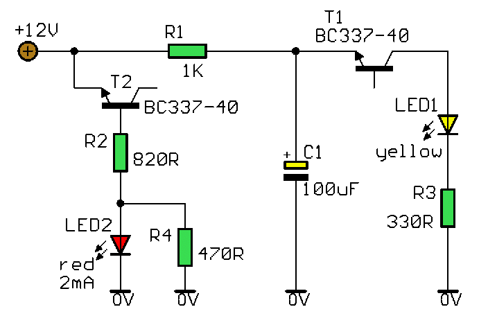
This simple and slightly odd circuit can clearly show the level of the supply voltage (in a larger device): as long as the indicator has good 12 volts at its input, LED1 gives steady, uninterrupted (for the naked eye) yellow light. If the input voltage falls below 11 V, LED1 will start to blink and the blinking will just get slower and slower if the voltage drops further - giving very clear and intuitive representation of the supplys status. The blinking will stop and LED1 will finally go out at a little below 9 volts. On the other hand, if the input voltage rises to 13 V, LED2 will start to glow, getting at almost full power at 14 V.

The characteristic voltages can be adjusted primarily by adjusting the values of R1 and R4.

The base-emitter diode of T2 basically just stands in for a zener diode. The emitter-collector path of T1 is inversely polarized and if the input voltage is high enough - T1 will cause oscillations and the frequency will be proportional to the input voltage. The relaxation oscillator ceases cycling when the input voltage gets so low that it no longer can cause breakdown along the emitter-collector path.

Not all small NPN transistors show this kind of behavior when inversely polarized in a similar manner, but many do. BC337-40 can start oscillations at a relatively low voltage, other types generally require a volt or two more. If experimenting, be careful not to punch a hole through the device under test: they oscillate at 9-12 V or not at all.
Source:www.zen22142.zen.co.uk
[Continue reading...]

Dome Lamp Dimmer circuit and explanation simple

- 0 comments

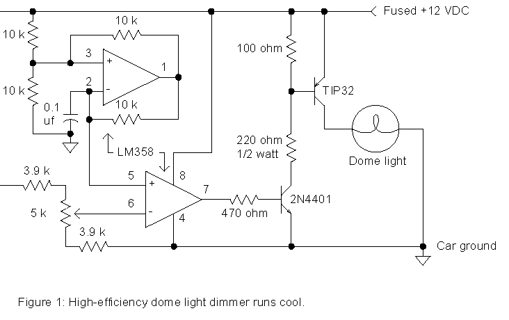
Many autos run power to lamps with only one wire using the car body for the return current path so the dimmer must interrupt the positive lead as shown. Simply cut the wire leading to the lamp and connect the lamp end to the collector of the TIP32 and connect the battery end to the circuit power input. Run an additional ground wire to the auto chassis from the circuit. This ground wire will not carry much current and may be a smaller gauge. There are times when a little light inside the car would greatly assist one of the passengers but the dome light is too bright for safe driving.

The dimmer circuit in fig. 1 may be added to an existing dome light or included with a new passenger spot lamp. The upper op-amp generates a 700 Hz sawtooth waveform which is compared to a setpoint voltage by the lower op-amp. When the sawtooth voltage is above the setpoint, the transistors turn on supplying current to the bulb. The setting of the potentiometer determines the width of the pulses sent to the lamp and therefore the average voltage. The lamp is dim when the potentiometer is set near the higher voltage. Since the TIP32 switches on and off instead of simply dropping the voltage like a power rheostat, the power it dissipates remains low and a heat sink is not necessary.
[Continue reading...]

Wednesday, October 8, 2014

12v battery charger using transistors circuit

- 0 comments

A very simple 12v battery charger circuit can be designed using a TIP3055 power transistor to limit the current to the battery by turning off when the battery voltage reaches approx 14v or if the current rises above 2 amp.

This battery charger electronic circuit is very simple and require few external electronic parts . Signal to turn off the TIP3055 transistor comes from two other transistors , the BC557 and BC 547. Firstly, the circuit turns on fully via the BD139 and TIP3055. The BC557 and BC 547 do not come into operation at the moment.
As the battery voltage rises, the voltage divider made up of the 1k8 and 39k creates a 0.65v between base and emitter of the BC557 and it starts to turn on at approx 14v.
The input voltage required by this charger electronic circuit project must be around 15 volts DC.

12v

[Continue reading...]

Sunday, October 5, 2014

TL494 200W ATX PC Power Supply

- 0 comments
Here I bring you wiring diagram of PCs power supply of DTK company. This power supply has ATX design and 200W performance. I was drawed diagram, when I repaired this power supply. This power supply circuit uses chip TL494. Similar circuit is used in the most power supplies with output power about 200W.Device use push-pull transistor circuit with regulation of output voltage.


TL494 200W ATX PC Power Supply Circuit

Line voltage goes through input filter circuit (C1, R1, T1, C4, T5) to the bridge rectifier. When voltage is switched from 230V to 115V, then rectifier works like a doubler. Varistors Z1 and Z2 have overvoltage protect function on the line input. Thermistor NTCR1 limits input current until capacitors C5 and C6 are charged. R2 and R3 are only for discharge capacitors after disconnecting power supply. When power supply is connected to the line voltage, then at first are charged capacitors C5 and C6 together for about 300V.

Then take a run secondary power supply controlled by transistor Q12 and on his output will be voltage. Behind the voltage regulator IC3 will be voltage 5V, which goes in to the motherboard and it is necessary for turn-on logic and for "Wake on something" functions. Next unstabilized voltage goes through diode D30 to the main control chip IC1 and control transistors Q3 and Q4. When main power supply is running, then this voltage goes from +12V output through diode D.

[Continue reading...]

Friday, October 3, 2014

5 Watt Class A Audio Amplifier

- 0 comments

On the day of the old valve, most commercial audio amplifiers suitable for compact integrated single discs or players used stereo amplifier topology of a single valve. The circuit is usually carried out through a multiple type valve, for example, a triode pentode ECL86.

Common features of the amplifiers are Class A operation, the output power in the 3 - 5W range, input sensitivity of about 600mV of total output power, THD of 3% @ 1KHz and 3W. Best types showed figures of 1.8% THD @ 3W and 0.8% @ 2W.

This solid-state push-pull single-ended Class A circuit is capable of providing a sound comparable to that of tube amplifiers, offering more output power (6.9W measured across a load of 8 ohm speaker cabinet), less THD, higher input sensitivity and better linearity.

Voltage and current for this circuit is 24 V and 700 mA, respectively, compared with 250 HT rail and 1A@6.3V heating filament of the valve works with amplifiers. The penalty only for the transistor circuit that works with the need for a larger heat sink for Q2 and Q3 (compared with the maximum power delivered). In any case, the amount of heat generated by this circuit can be comparable to that of a single valve amplifier. A choice of low-boost facility can be added through R5 and C5.

This circuit was built and compared with a circuit of a valve box phonograph in the early 1950 by Aren van Waard, a Dutch biochemist working in the field of medical imaging (PET) with a strong interest in audio amplifiers valve. A complete description of the circuits and test results of subjective comparisons made by the distinguished author appeared in the magazine AudioXpress: February, March and April 2005 issues.
[Continue reading...]

Tone Detector circuit diagrams and explanation

- 0 comments

The following circuit diagrams are tone detector circuit diagrams which also known as sound activated switch circuit. Actually, these circuits use micro-controller for switching because the circuits were designed for robot start up activation. But you can build switching module using relay.

Tone Detector diagram 1

Tone

Tone Detector diagram 2

Tone

Tone Detector diagram 3

Tone

Tone Detector diagram 4

Tone

Tone Detector diagram 5

Tone

Source: Sound activated switch for robot

[Continue reading...]

Thursday, October 2, 2014

Simplest Single Phase Preventor Circuit for Three Phase Motor Potection

- 0 comments
 For a 3-phase induction motor,Lit is necessary that all the three phases of supply are present while it is on load.
When any one of the fuses goes out, or a phase is missing, the motor will continue to run with two phases only, but it will start drawing a huge current for the same load.

This high current may ruin the motor, unless switched off immediately. A single phase preventor circuit avoids such a mishap. With this circuit the motor will not run, unless all the three phases are present. In a 3-phase supply, the voltages are 120 degrees apart from each other. Thus the addition of three phases gives zero voltage. lf any one of the phase goes, voltage present at the summing point equals half the line voltage. ‘ In this circuit, the three phases (R, Y, B) are connected to line neutral, which in turn is connected to the ground of the   circuit.

When all three phases are present, voltage at point D is zero. So potential at pin 3 of 1C 741 is also zero, but voltage at pin 2 is nearly 4V. Here 741 is used as a comparator and the voltage at pin 6 is zero. Hence the relay cannot operate. When a phase goes out, voltage at point D goes up to about halt the line voltage. This voltage is divided by 150k and 50k resistors. The voltage at pin 3 is about 8V when 50k potentiometer is properly adjusted. The voltage at pin 6 is about 12V. This base voltage can drive the relay into operating condition. So, the relay would operate when any of the phases goes out.  This relay, when used in the control circuit of the 3-phase motor, or with a circuit breaker, would switch the power oft on operation.


[Continue reading...]
 
Copyright © 2012. Fast Diagrams - Posts · Comments
Powered by Blogger