Friday, September 26, 2014

Flashlight Controlled Remote Control Switch Circuit

- 0 comments
It is sometimes very annoying for a person who, while watching a TV programme or listening to a radio or the like, has to get up to switch lights or fans or AC off. The same applies when he wants to switch them on.
Using the simple flashlight remote control circuit shown in Fig. 1, one can switch almost any domestic electrical equipment from a distance, simply by flashing a torchlight.  The basic sensor used in this remote switching mechanism - is a light dependent resistor (LDR), whose resistance value changes in response to the incident light. The 555 timer is used in the monostable mode in Fig. 1, which is triggered when the voltage at its pin 2 falls below l/3 Vcc. This triggering takes place when light is incident on the LDR, thus lowering its resistance value. The l0k pot VRI is used  for setting up the triggering threshold.

The output time  period of the 555 is adjustable up to l2 seconds by varying the 500k pot VR2, so as to smooth up the light impulse (similar to switch debouncing); The output of the 555 is fed to the input ofa JK master/slave flip-flop (7473) which is configured in the toggle mode (by tying the J and K inputs to Vcc). ln the toggle mode, the output of the flip-flop changes state with every pulse at its clock input. The output of the 7473 feeds an amplifier stage comprising a BC 148 and a SLl00 transistor which are used to drive a relay that switches the instrument to be controlled. The circuit can be mounted on a small veroboard and placed in a cabinet with a small hole for exposing the LDR. Care should be taken to ensure that the LDR receives only the light from the torch, and that no ambient light falls on it. Once so installed, it will work reliably, with no false triggering that sometimes occurs in sound operated remote control units.

The entire digram for the flashight controlled remote circuit is shown below:


[Continue reading...]

Thursday, September 25, 2014

Simple Time Delay Circuit Using Op Amp

- 0 comments
lC1a is provided with re- sistive and capacitive feedback to form an integrator with initial conditions. lC1b is in an "open loop" mode so that its output is either high or low depending on its inputs, and changes state when the output of lC1a goes more negative than the voltage set at ZD2.
When . the output of IC1 b goes positive the transistor Q1 biases hard on switching the SCR on. Diodes D1 -D4 are to make the SCR conduct on both halves of the mains wave form. The delay period is set by the components ZD1, ZD2;·C, RVl, and  R. lf ZD1 is chosen to be OV5 and ZD2 at 5V, then the maximum delay period is given by T= 10CR
RV1 = ZD2/ZD1 * R<10.r

 The meter is a voltrneter with as fsd equal to the value of ZD2. The switch then operates when the meter reaches fsd. The meter can therefore be calibrated to show remaining delay with OV equal to T and fsd equal to zero. SW2 changes round the inputs of the op—amp so that the output either swings from high to low, or, low to high. SW3 is to reset the time delay which it does by discharging the capacitor. ZD3 should be chosen  to be a value slightly higher than ZD2, this is to stop the capacitor charging beyond a set limit and therefore overloading the meter. SW1 is the run—hold switch. When the switch is at +12 volts the integrator charges the capacitor. When the switch is set to OV the charging of the capacitor is stopped until the switch is set back to 12 volts. . Q1 is a buffer to avoid loading on the IC and to trigger the SCR. The supply voltage should be 12-0-12 and does not need to be well smoothed as the zener diodes set the timing function,


Simple Time Delay Circuit Using Op Amp


[Continue reading...]

Economical Switching LED Driver Circuit

- 0 comments
The usual method of operating an LED from a voltage which is higher than its forward voltage is well known. A limiting resistor is used to limit the LED current to its rated value. Learn how to make an economical LED driver circuit.
Calculating the value of the  resistor is simple enough: supply  voltage minus LED forward voltage divided by the maximum current rating of the LED. The formula is: Thus the voltage difference between supply voltage and forward voltage  is dropped by the limiting resistor. However, the disadvantage is that the power dissipated by the limiting resistor is fairly high if the supply  voltage is relatively high. Thus, for  example, with a supply voltage of 24 V and a current of 25 mA the power dissipated is greater than 0.5 W. There is an alternative: the circuit shown here only requires 0.1 W. lt is effectively a switched current source. The current source is based on transistor T1 and the oscillator uses a 3140 operational amplifier.

When transistor T1 conducts, a current flows via coil L1, LED D1 and resistor R3 to earth. The current curve is shown in figure 2. As soon as T1 turns on and a current flows, the current rises together with the volt- age at R3 from zero volts. This voltage is now applied to the non- inverting input of the operational amplifier. A reference voltage of approximately 0.25 V is applied via voltage divider Rl/R2 to the inverting input. lf the rising voltage at the non-inverting input reaches the level of the reference voltage, the output of the operational amplifier switches to a high voltage potential. Transistor T1 turns off and the current through the LED flows via diode D2. As shown in figure 2, the current drops; the voltage at R3 therefore drops also. Once the current and voltage are sufficiently low, the operational amplifier switches over again and the transistor turns on.

This operation is repeated periodically. The switching point is adjusted with preset potentiometer P1. This governs the changeover voltage at pin 3 of the operational amplifier which, in turn, governs the maximum LED current. lt should not exceed 50 mA. The frequency of the oscillator (which is also the switching frequency for the transistor) is deter- mined by coil L1 and by the switching hysteresis adjusted with P 1. With the specified value of 4.7mH the switching frequency is about 15 kHz with a period of approximately 65 ps. Two other switching frequencies using different coil inductances can be found in the following table: Coil T F 2.2 mH 35 ,us 30 kHz 10 mH 150,is 6kHz P1 should be adjusted to obtain the lowest frequency at which the circuit still starts to oscillate.


[Continue reading...]

Wednesday, September 24, 2014

Simple Tachometer Circuit or Revolution Counter Circuit

- 0 comments
The explained idea of a simple tachometer circuit can be used as a revolution counter tester for determining or setting the correct optimal engine speed which may ensure maximum engine efficiency from the vehicle. The pulses emanating from the contact breaker are shaped and limited by Fl2/R5/ D2. Transistor T2 conducts only when the contact breaker is open, because the full battery voltage is then present at the input (PL2) of the rev counter (see figure 48). Capacitor C2 is then discharged rapidly through R6 and T2. When T2 is cut off when the contact breaker closes, C2 charges only slowly via R4.

This ensures that the trailing edge caused by the closing of the contact breaker is applied to the next stage as a steep pulse, while the noise spikes are suppressed by the slow charging of C2. It follows that C2 must be carefully matched to the particular car engine. Diodes D4 and D5 protect the trigger input of IC1 against too high positive and negative voltages. The real heart of the circuit is C1: this versatile counter is connected as a monostable multivibrator (MMV). After every trigger pulse at pin 2 (negative voltage jump applied via C4) it generates an output pulse of constant period which may be preset with P1. Unfortunately, the counter auto-triggers if pin 2 is still logic low after the output pulse period has lapsed, and because of that R8 ensures that C4 can only pass very narrow trigger pulses.

The resistor and capacitor form a so called differentiating network (see figure 49).  It would now be possible to connect a suitable moving-coil meter to the output (pin 3) of IC1. Because of the inertia of this instrument, the individual output pulses (pulse width = O.7C7 (P1+R11) sec) are averaged (integrated). The meter reading corresponds exactly to the average value of the pulse height (see figure 50) and is therefore  provided Pl has been adjusted correctly proportional to the instantaneous engine speed.

The comparator, A3, following IC1 has no inertia and the output pulses from IC1 must therefore be smoothed’: this is effected by two integrating networks, R7/C5 and R9/C8 (see figure 51). Across C8 there exists therefore a reasonably constant direct voltage (the remaining ripple caused by the original pulses may be ignored) which is directly proportional to the engine speed (see figure 52). This direct voltage is set to 5 V at maximum engine speed during the calibration which follows later.

The following image shows the simple tachometer circuit design


The waveform images can be verified from the folowing images.


[Continue reading...]

Tuesday, September 23, 2014

Digital Remote Thermometer

- 0 comments

Remote sensor sends data via mains supply
Temperature range: 00.0 to 99.9 °C

Transmitter circuit diagram:

Transmitter parts:
R1,R3 100K 1/4W Resistors
R2 47R 1/4W Resistor
R4 5K 1/2W Trimmer Cermet
R5 12K 1/4W Resistor
R6 10K 1/4W Resistor
R7 6K8 1/4W Resistor
R8,R9 1K 1/4W Resistors
C1 220nF 63V Polyester Capacitor
C2 10nF 63V Polyester Capacitor
C3 1µF 63V Polyester Capacitor
C4,C6 1nF 63V Polyester Capacitors
C5 2n2 63V Polyester Capacitor
C7,C8 47nF 400V Polyester Capacitors
C9 1000µF 25V Electrolytic Capacitor
D1 1N4148 75V 150mA Diode
D2,D3 1N4002 100V 1A Diodes
D4 5mm. Red LED
IC1 LM35 Linear temperature sensor IC
IC2 LM331 Voltage-frequency converter IC
IC3 78L06 6V 100mA Voltage regulator IC
Q1 BC238 25V 100mA NPN Transistor
Q2 BD139 80V 1.5A NPN Transistor
L1 Primary (Connected to Q2 Collector): 100 turns
Secondary: 10 turns
Wire diameter: O.2mm. enameled
Plastic former with ferrite core. Outer diameter: 4mm.
T1 220V Primary, 12+12V Secondary 3VA Mains transformer
PL1 Male Mains plug & cable

Receiver circuit diagram:

Receiver Parts:
R1 100K 1/4W Resistor
R2 1K 1/4W Resistor
R3,R4,R6-R8 12K 1/4W Resistors
R5 47K 1/4W Resistor
R9-R15 470R 1/4W Resistors
R16 680R 1/4W Resistor
C1,C2 47nF 400V Polyester Capacitors
C3,C7 1nF 63V Polyester Capacitors
C4 10nF 63V Polyester Capacitor
C5,C6,C10 220nF 63V Polyester Capacitors
C8 1000µF 25V Electrolytic Capacitor
C9 100pF 63V Ceramic Capacitor
D1,D2,D5 1N4148 75V 150mA Diodes
D4,D4 1N4002 100V 1A Diodes
D6-D8 Common-cathode 7-segment LED mini-displays
IC1 4093 Quad 2 input Schmitt NAND Gate IC
IC2 4518 Dual BCD Up-Counter IC
IC3 78L12 12V 100mA Voltage regulator IC
IC4 4017 Decade Counter with 10 decoded outputs IC
IC5 4553 Three-digit BCD Counter IC
IC6 4511 BCD-to-7-Segment Latch/Decoder/Driver IC
Q1 BC239C 25V 100mA NPN Transistor
Q2-Q4 BC327 45V 800mA PNP Transistors
L1 Primary (Connected to C1 & C2): 10 turns
Secondary: 100 turns
Wire diameter: O.2mm. enameled
Plastic former with ferrite core. Outer diameter: 4mm.
T1 220V Primary, 12+12V Secondary 3VA Mains transformer
PL1 Male Mains plug & cable

Device purpose:
This circuit is intended for precision centigrade temperature measurement, with a transmitter section converting to frequency the sensors output voltage proportional to the measured temperature. The output frequency bursts are conveyed into the mains supply cables.
The receiver section counts the bursts coming from mains supply and shows the counting on three 7-segment LED displays. The least significant digit displays tenths of degree and then a 00.0 to 99.9 °C range is obtained.
Transmitter-receiver distance can reach hundred meters, provided both units are connected to the mains supply within the control of the same light-meter.

Transmitter circuit operation:
IC1 is a precision centigrade temperature sensor with a linear output of 10mV/°C driving IC2, a voltage-frequency converter. At its output pin (3), an input of 10mV is converted to 100Hz frequency pulses. Thus, for example, a temperature of 20°C is converted by IC1 to 200mV and then by IC2 to 2KHz. Q1 is the driver of the power output transistor Q2, coupled to the mains supply by L1 and C7,C8.

Receiver circuit operation:
The frequency pulses coming from mains supply and safely insulated by C1,C2 & L1 are amplified by Q1; diodes D1,D2 limiting peaks at its input. Pulses are filtered by C5, squared by IC1B, divided by 10 in IC2B and sent for the final count at the clock input of IC5.
IC4 is the time-base generator: it provides reset pulses for IC1B and IC5 and enables latches and gate-time of IC5 at 1Hz frequency. It is driven by a 5Hz square wave obtained from 50Hz mains frequency picked-up from T1 secondary, squared by IC1C and divided by 10 in IC2A.
IC5 drives the displays cathodes via Q2,Q3 & Q4 at a multiplexing rate frequency fixed by C7. It drives also the 3 displays paralleled anodes via the BCD-to-7 segment decoder IC6.
Summing up, input pulses from mains supply at, say, 2KHz frequency, are divided by 10 and displayed as 20.0°C.

Notes:
D6 is the Most Significant Digit and D8 is the Least Significant Digit.
R16 is connected to the Dot anode of D7 to permanently light the decimal point.
Set the ferrite cores of both inductors for maximum output (best measured with an oscilloscope, but not critical).
Set trimmer R4 in the transmitter to obtain a frequency of 5KHz at pin 3 of IC2 with an input of 0.5Vcc at pin 7 (a digital frequency meter is required).
More simple setup: place a thermometer close to IC1 sensor, then set R4 to obtain the same reading of the thermometer in the receivers display.
Keep the sensor (IC1) well away from heating sources (e.g. Mains Transformer T1).
Linearity is very good.


author: RED Free Circuit Designs
e-mail:
web site: http://www.redcircuits.com
[Continue reading...]

Monday, September 22, 2014

12 Volt 30 Amp PSU circuit and explanation

- 0 comments

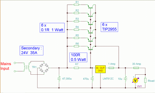
Using a single 7812 IC voltage regulator and multiple outboard pass transistors, this power supply can deliver output load currents of up to 30 amps. The design is shown below:

Circuit diagram

Notes:
The input transformer is likely to be the most expensive part of the entire project. As an alternative, a couple of 12 Volt car batteries could be used. The input voltage to the regulator must be at least several volts higher than the output voltage (12V) so that the regulator can maintain its output. If a transformer is used, then the rectifier diodes must be capable of passing a very high peak forward current, typically 100amps or more. The 7812 IC will only pass 1 amp or less of the output current, the remainder being supplied by the outboard pass transistors. As the circuit is designed to handle loads of up to 30 amps, then six TIP2955 are wired in parallel to meet this demand. The dissipation in each power transistor is one sixth of the total load, but adequate heat sinking is still required. Maximum load current will generate maximum dissipation, so a very large heat sink is required. In considering a heat sink, it may be a good idea to look for either a fan or water cooled heat sink. In the event that the power transistors should fail, then the regulator would have to supply full load current and would fail with catastrophic results. A 1 amp fuse in the regulators output prevents a safeguard. The 400mohm load is for test purposes only and should not be included in the final circuit. A simulated performance is shown below:

Calculations:
This circuit is a fine example of Kirchoffs current and voltage laws. To summarise, the sum of the currents entering a junction, must equal the current leaving the junction, and the voltages around a loop must equal zero. For example, in the diagram above, the input voltage is 24 volts. 4 volts is dropped across R7 and 20 volts across the regulator input, 24 -4 -20 =0. At the output :- the total load current is 30 amps, the regulator supplies 0.866 A and the 6 transistors 4.855 Amp each , 30 = 6 * 4.855 + 0.866. Each power transistor contributes around 4.86 A to the load. The base current is about 138 mA per transistor. A DC current gain of 35 at a collector current of 6 amp is required. This is well within the limits of the TIP2955. Resistors R1 to R6 are included for stability and prevent current swamping as the manufacturing tolerances of dc current gain will be different for each transistor. Resistor R7 is 100 ohms and develops 4 Volts with maximun load. Power dissipation is hence (4^2)/200 or about 160 mW. I recommend using a 0.5 Watt resistor for R7. The input current to the regulator is fed via the emitter resistor and base emitter junctions of the power transistors. Once again using Kirchoffs current laws, the 871 mA regulator input current is derived from the base chain and the 40.3 mA flowing through the 100 Ohm resistor. 871.18 = 40.3 + 830. 88. The current from the regulator itself cannot be greater than the input current. As can be seen the regulator only draws about 5 mA and should run cold.


author:
e-mail:
web site: http://www.mitedu.freeserve.co.uk/
[Continue reading...]

Fuse Box Toyota 1987 Truck Under Dash Diagram

- 0 comments
Fuse Box Toyota 1987 Truck Under Dash Diagram - Here are new post for Fuse Box Toyota 1987 Truck Under Dash Diagram.

Fuse Box Toyota 1987 Truck Under Dash Diagram


Fuse
Fuse

Fuse Panel Layout Diagram Parts: wiper, engine, ignition switch, cigar lighter, power window, door lock, stop lamp, defogger relay, turn signal flasher, main relay, teillight relay, taillight.
[Continue reading...]

Sunday, September 21, 2014

Dual Mode Battery Charger Circuit

- 0 comments

There are two main types of battery charger – constant voltage and constant current. Both have their advantages and disavantages. For constant voltage, the battery cannot be overcharged but the charging rate is slow. Constant current mode can charge batteries more swiftly but there is the danger of overcharging them.

The dual mode battery charger circuit featured here was designed to combine both modes, but without their disadvantages, for use with a 6V sealed lead-acid battery. The main players of the circuit are voltage regulator IC1, which is used for constant current mode, and precision adjustable shunt regulator IC2, which is used for constant voltage mode.

In constant current mode, resistor R4 sets the current at 370mA, according to the equation:
R4 = (1.25/I) x 1000
where I = the constant current required, in milliamps.

Circuit diagram :

Dual Mode Battery Charger Circuit Diagram

Diode D3 prevents the battery from discharging back into IC1 if the input supply is disconnected. Resistor R3 provides current to switch one transistor TR1 when the input supply is present. Shunt regulator IC2, resistors R6, R7 and preset potentiometer VR1 form the network which determines whether on not the battery has reached its required voltage. When the voltage at IC2′s reference input reaches 2.5V, IC2 switches on its internal transistor, connecting IC1′s ADJ (adjust) pin to 0V. In this condition, IC2 holds IC1 in constant current supply mode. Capacitor C3 helps to stabilise the switching of IC2.

Capacitor C1 and C2 decouple the DC input supply voltage. Light emitting diode D1 is a power-on indicator, and LED D2 is turned on when constant voltage mode is activated. A heatsink may be needed with IC1. In use, adjust preset VR1 so that the voltage at the output suits the peak voltage required by the sealed lead-acid battery,which is usually printed on its body. Once adjusted correctly, it should not need further adjustment.

The authos used a 12V 600mA DC adapter for powering the dual mode battery charger circuit. The battery with which it is used has a peak voltage range of 6.9V to 7.12V.

[Continue reading...]

Saturday, September 20, 2014

Subwoofer circuit

- 0 comments
Circuit Descrition
The acoustic spectrum is extended by very low frequencies 20Iz and reaches as the 20000Iz in high frequencies. In the low frequencies is degraded the sense of direction. This reason us leads to the utilization speaker for the attribution of very low frequencies. The manufacture that to you we propose distinguishes these frequencies, in order to him we lead to the corresponding amplifier. The acoustic filters are met in various points in the sound systems. The knownest application they are the filters baxandal for regulating tone low and high frequencies and filters crossover where the acoustic region is separated in subareas, in order to it leads the corresponding loudspeakers. The application that to you we propose is a simple filter of region that limits the acoustic region (20-20000Hz) in the region 20-100Hz.

With the manufacture that to you we propose you can make a active filter in order to you lead a loudspeaker of very low frequencies. With this you will place one bigger speaker between the HIFI speakers of you. In order to you have a complete picture of sound you will need also the corresponding amplifier. In the entry of circuit you will connect the two exits of preamplifier or the exit of line of some preamplifier. The circuit of manufacture allocates a exit in order to is led means of circuit of force subwoofer. If for some reason you do not have space in order to you place the third speaker in space of hearing, then you can select smaller speaker. The output will depend from the type of music that you hear. If in deed you have space, then after you make a filter and remain thanked, you can him recommend in your friends or still make other same for your friends.


Circuit Diagram


In the form it appears the theoretical circuit of filter. In first glance we see three different circuits that are mainly manufactured round two operational amplifiers. This circuits constitute mixed, amplifier with variable aid and a variable filter. The manufacture end needs a circuit of catering with operational tendency of catering equal with ±12. the operational amplifiers that constitute the active elements for this circuits of are double operational type as the TL082 and NE5532. The operational these amplifiers belong in a family provided with transistor of effect of field IFET in their entries. Each member of family allocates in their circuit bipolar transistor and effect of field. This circuits can function in his high tendency, because that they use transistor of high tendency. Also they have high honor of rhythm of elevation (slew rate), low current of polarization for the entries and are influenced little by the temperature. The operational these amplifiers have breadth of area unity gain bandwidth 3MHz. A other important element for their choice is the big reject of noise, when this exists in the line of catering.

The price of reject is bigger than 80dB, their consumption is small, from 11 until 3 mA. They are internally sold in nutshell with eight pins and allocate two operational amplifiers, In the same line in nutshell 14 pins they incorporate four operational, In the trade they are sold with code TL074, TL084 and TL064, In nutshell with eight pins they are sold operational amplifiers TL061 TL071 kajTL081. In the manufacture we used the TL082 that has two operational. First operational from the TL082 it works as amplifier and mixed for the two channels, In his negative entry he exists one small mixed with two resistances. A potentiometer in this rung determines the aid of circuit. In the point this left winger and the right channel of preamplifier they are added means of two resistances. En continuity the operational strengthens signal with aid made dependent from the price that has the potentiometer.

The place of runner is proportional with the aid of circuit. The second operational amplifier is the filter of manufacture. The filter of is acoustic frequency of second class and he is made with the materials that are round the operational amplifier. The filter of is low passage with variable frequency of cutting off. This frequency can be altered and take prices from very low frequency the 30Hz or still exceed 150Hz. The frequency of cutting off of filter depends from the prices that have the elements of circuit. Altering the values of elements we can have frequency of cutting off 150Iz, 130Iz, J00Iz, 7Ïz, 6Íz even 3Íz, this prices they can be achieved with the simple rotation of double potentiometer. The circuit of filter has been made around one operational that it has completed TL082 that is double operational amplifier. In the exit of filter we will link the plug of expense where is connected the amplifier. In the exit of circuit is presented, the limited as for the breadth of frequencies, signal that we apply in the entry of circuit.

Parts

R1 = 39 Kohm
R2 = 39 Kohm
R3 = 47 Kohm
R4 = 10 Ohm
R5 = 22 Kohm
R6 = 4,7 Kohm
R7 = 22 Kohm
R8 = 4,7 Kohm
R9 = 10 Ohm
R10 = 220 Ohm
C1 = 39 pF
C2 = 0.1 uF
C3 = 0.1 uF
C4 = 0.2 uF
C5 = 0.4 uF
C6 = 0.1 uF
C7 = 0.1 uF
IC1 = TL064

PCB and layout


In order to you make the manufacture you will need printed that appears in the form. In this you will place the materials according to the following form. The materials are enough also easy can become certain errors. With few attention however you can him avoid. If they are presented difference malfunctions, you check carefully the circuit. The circuit, as we said, is filter and it should they are used materially good precision and quality, particularly for the capacitors. The capacitors of filters will have tolerance 5%. Of course, the manufacture will also work with material of lower quality, the trial of manufacture can become with acoustic signal of generator We apply the generator in the entry of manufacture and we measure with a voltmeter the tendency in the exit of filter. If we alter the potentiometer and are altered the tendency, then all have well.

Original article sourse: diy-electronic-projects.com

[Continue reading...]

Friday, September 19, 2014

VIEWSONIC G90fB 4 Model No VS10794 19” Digital Controlled Color Monitor Schematic Full

- 0 comments
Viewsonic G90fB-4 Model No. VS10794 - 19” Digital Controlled Color Monitor_Circuit Diagram_[Full]
CPU 
SMPS
OUTPUT
VIDEO

[Continue reading...]

Ultrasonic Distant Obstacle Detector

- 0 comments
The first sensor a robot usually gets fitted with is an obstacle detector. It may take three different forms, depending on the type of obstacle you want to detect and also — indeed, above all — on the distance at which you want detection to take place. For close or very close obstacles, reflective IR sensors are most often used, an example of such a project appears elsewhere in this blog. These sensors are however limited to distances of a few mm to ten or so mm at most. Another simple and frequently-encountered solution consists of using antennae-like contact detectors or ‘whiskers’, which are nothing more than longer or shorter pieces of piano wire or something similar operating microswitches.

Circuit diagram:

Ultrasonic
Ultrasonic Distant Obstacle Detector Circuit Diagram

Detection takes place at a slightly greater distance than with IR sensors, but is still limited to a few cm, as otherwise the whiskers become too long and hinder the robot’s normal movement, as they run the risk of getting caught up in things around it. For obstacles more than a couple of cm away, there is another effective solution, which is to use ultrasound. It’s often tricky to use, as designers think as if they needed to produce a telemeter, when in fact here we’re just looking at detecting the presence or absence of obstacles, not measuring how far away they are. So here we’re suggesting an original approach that makes it possible to reduce the circuit required to a handful of cheap, ordinary components.

 ultrasonic distant obstacle detector Our solution is based on the howlround or feedback effect all too familiar to sound engineers. This effect, which appears as a more or less violent squealing, occurs when a microphone picks up sound from speakers that are connected to it via an amplifier. Feeding back the output signal from the speaker into the input (the microphone) in this way creates an acoustic oscillator. Our detector works on the same principle, except that the microphone is an ultrasound receiver while the speaker is an ultrasonic emitter. They are linked just by a very easily-built ordinary amplifier. Feedback from the output to the input occurs only when the ultrasonic beam is reflected off the obstacle we are trying to detect.
As Figure 1 shows, the receiver RXUS is connected to the input of a high-gain amplifier using transistors T1 and T2. As the gain of this stage is very high, it can be reduced if necessary by pot P1 to avoid its going into oscillation all on its own, even in the absence of an obstacle. The output of this amplifier is connected to the ultrasonic emitter TXUS, therby forming the loop that is liable to oscillate due to the effect of feedback. When this takes place, i.e. when an obstacle is close enough to the ultrasonic transducers, a pseudo-sine wave signal at their resonant frequency of 40 kHz appears at the amplifier output, i.e. at the terminals of the transmitting transducer.

This signal is rectified by D1 and D2 and filtered by C3 and, if its amplitude is high enough, it produces a current in R6 capable of turning transistor T3 on to a greater or lesser extent. Depending on the nature and distance of the obstacle, this process does not necessarily happen in a completely on/off manner, and so the level available at T3 collector may be quite poorly-defined. The Schmitt CMOS invertors are there to convert it into a logic signal worthy of the name. So in the presence of an obstacle, S1 goes high and S2 goes low. Powering can be from any voltage between 5 and 12 V.

The gain, and hence the circuit’s detection sensitivity, does vary a bit with the supply voltage, but in all cases P1 makes it possible to achieve a satisfactory setting. Although it is very simple, under good conditions this circuit is capable of detecting a normally-ultrasound-reflective obstacle up to around 5 or 6 cm away. If a smaller distance is needed, you simply have to reduce the gain by adjusting P1. Building the circuit is straightforward. Both transducers are 40 kHz types that can be found in any retailers, and the other components couldn’t be more ordinary.  in Figure 2.
[Continue reading...]

Thursday, September 18, 2014

Mercedes Explanation Fuse Box Year 2000 230 Fuel Injection Diagram

- 0 comments
Fuse Box Mercedes 2000 230 Fuel Injection Diagram - Below is Fuse Box Mercedes 2000 230 Fuel Injection Diagram.

Fuse Box Mercedes 2000 230 Fuel Injection Diagram


Fuse
Fuse

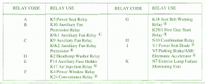
Fuse Panel Layout Diagram Parts: power seat, auxiliary fan, preresistor, headlamp washer relay, auxiliary fuse holder, air injection relay, power window relay, convenience relay, seat belt warning, gear start relay, combination relay, parking brakke, exterior lamp
[Continue reading...]

Wednesday, September 17, 2014

Dual Regulated Power Supply

- 0 comments

In this circuit, the 7815 regulatates the positive supply, and the 7915 regulates the negative supply. The transformer should have a primary rating of 240/220 volts for europe, or 120 volts for North America.

Dual Regulated Power Supply Circuit diagram :

The centre tapped secondary coil should be rated about 18 volts at 1 amp or higher, allowing for losses in the regulator. An application for this type of circuit would be for a small regulated bench power supply.

[Continue reading...]

12 12W STEREO AMPLIFIER WITH MUTING

- 0 comments
12 +12W STEREO AMPLIFIER WITH MUTING


[Continue reading...]

Tuesday, September 16, 2014

Phone Line Polarity Checker

- 0 comments
Do you suspect your broadband speed (DSL) is slower than it should be? It could be as simple as incorrect polarity in your phone wall socket. Build this very cheap, very simple device to find out whether you need to change your wiring!

It might not seem that telephone line polarity is important, since the ring and voice signals sent over telephone lines are AC. However the lines are actually biased to 48V DC (less when in use) and so the polarity can matter. The main problem with incorrect polarity is that some DSL (Digital Subscriber Line) modems and routers can perform poorly in this circumstance. Since telephone wires are color-coded, it should be possible to simply check that the sockets are wired correctly. Unfortunately, there are multiple wiring colour schemes and they have changed over time. Believe it or not, the old color scheme (from around 15 years ago) is identical to the current colour scheme except that the polarity of both lines is reversed! This is why so many homes have this problem and yours may well be one of them.

PhoneThe common telephone line is simply a copper pair, ie, two wires. As mentioned, there is usually a 48V DC bias across the pair which drops to around 8V when a telephone is “off-hook”. The ring voltage (around 90V AC) and the audio signal voltage (also AC) are overlaid on this DC bias. The DC power is “rectified” by each telephone on that line to run its own circuitry. Note, though, that this does not include cordless phones which usually use a plugpack, as their power requirements are far in excess of what the telephone line can deliver. (As an aside, that is the reason it is important to keep a line-powered telephone in your home so you can still make and receive calls if the mains power goes out.

PhoneTelephone exchanges can usually supply power from their backup batteries for up to some days, even if they are blacked out). Usually, telephone lines are run with 4-core cable. This allows up to two lines on the one cable. The first line is on the inner pair (pins 2 and 3) and the second line, if present, is on the outer pair (pins 1 and 4). Modern telephones use modular plugs, specifically RJ11 (6P2C, one line), RJ14 (6P4C, one or two lines) or RJ25 (6P6C, 1-3 lines). By the way, 6P4C stands for “six pins, four connectors”. Incidentally, “RJ12” connectors are physically compatible – and commonly available – so that is what we have used in this project.

PhoneBecause modern phones rectify the DC voltage from the telephone lines before regulating it and because the ring and voice signals are AC, for voice communications the polarity doesn’t really matter.
[Continue reading...]

Monday, September 15, 2014

VGA to BNC Adapter Converter Wiring diagram Schematic

- 0 comments
There are monitors which only have three BNC inputs and which use composite synchronization (‘sync on green’). This schema has been designed with these types of monitor in mind. As can be seen, the schema has been kept very simple, but it still gives a reasonable performance. The principle of operation is very straightforward. The RGB signals from the VGA connector are fed to three BNC connectors via AC-coupling capacitors. These have been added to stop any direct current from entering the VGA card. A pull-up resistor on the green output provides a DC offset, while a transistor (a BS170 MOSFET) can switch this output to ground. It is possible to get synchronisation problems when the display is extremely bright, with a maximum green component.

In this case the value of R2 should be reduced a little, but this has the side effect that the brightness noticeably decreases and the load on the graphics card increases. To keep the colour balance the same, the resistors for the other two colors (R1 en R3) have to be changed to the same value as R2. An EXOR gate from IC1 (74HC86) combines the separate V-sync and H-sync signals into a composite sync signal. Since the sync in DOS-modes is often inverted compared to the modes commonly used by Windows, the output of IC1a is inverted by IC1b. JP1 can then by used to select the correct operating mode. This jumper can be replaced by a small two-way switch, if required.

VGA-to-BNC VGA-to-BNC
   partspcb

This switch should be mounted directly onto the PCB, as any connecting wires will cause a lot of interference. The PCB has been kept as compact as possible, so the schema can be mounted in a small metal (earthed!) enclosure. With a monitor connected the current consumption will be in the region of 30 mA. A 78L05 voltage regulator provides a stable 5 V, making it possible to use any type of mains adapter, as long as it supplies at least 9 V. Diode D2 provides protection against a reverse polarity.

LED D1 indicates when the supply is present. The schema should be powered up before connecting it to an active VGA output, as otherwise the sync signals will feed the schema via the internal protection diodes of IC1, which can be noticed by a dimly lit LED. This is something best avoided.

Resistors:
R1,R2,R3 = 470Ω
R4 = 100Ω
R5 = 3kΩ3


Capacitors:
C1,C3,C5 = 47µF 25V radial
C2,C4,C6,C7,C10 = 100nF ceramic
C8 = 4µF7 63V radial
C9 = 100µF 25V radial


Semiconductors:
D1 = LED, high-efficiency
D2 = 1N4002
T1 = BS170
IC1 = 74HC86
IC2 = 78L05


Miscellaneous:
JP1 = 3-way pinheader with jumper
K1 = 15-way VGA socket (female), PCB mount (angled pins)
K2,K3,K4 = BNC socket (female), PCB mount, 75Ω    .
[Continue reading...]

Sunday, September 14, 2014

SCHEMA CONVERTER AC 12VDC 220VAC

- 0 comments

CMOS 4047 is the capital basic of this baby voltage advocate which transforms a 12V dc into 220V ac. 4047 is acclimated as a astable mutivibrator, at pins 10 and 11 will accept a balanced ellipsoidal arresting wich is amplified b 2 Darlington transistors and assuredly ability the accessory braid of mains agent ( 2×10V / 60VA ).

At the capital braid terminals will get 220V. With the advice of P1 the achievement frequnecy can be adapted amid 50Hz to 400Hz. Although this is not allotment of any able dc ac converters it can be acclimated absolutely able on some home appliances.

[Continue reading...]

12v Battery Charger Circuit

- 0 comments
The schema may be accustomed charge 12V lead acid batteries.

Overview

Pin one of the LM317 IC is that the management pin that is employed to manage the charging voltage, Pin a pair of is that the output at that the charging voltage seems, Pin three is that the input to that the regulated DC offer is given.

The charging voltage and current is controlled by the electronic transistor (Q1), electrical device (R1) and POT (VR1). once the battery is 1st connected to the charging terminals, the present through R1 will increase. This successively will increase the present and voltage from LM317. once the battery is totally charged the charger reduces the charging current and also the battery are charged within the trickle charging mode.

Circuit


Notes
  • The input voltage to the schema should be a minimum of 3V more than the expected output voltage. luminous flux unit 317 dissipates around 3V throughout its operation. Here I used 18V DC because the input.
  • The charging voltage may be set by victimization the POT (VR1).
  • The luminous flux unit 317 should be mounted on a sink.
  • All capacitors should be rated a minimum of 25V.
  • Youll be able to use crocodilian clips for connecting the battery to the charger.
[Continue reading...]

Saturday, September 13, 2014

Small Surround Sound Decoder

- 0 comments
Small

This is surround sound decoder. With this schema, you can divide the 2 channel (R and L channel) stereo output become 4 channel output that are R channel, L channel, Center out and Rear out. This schema will enrich your audio sound system.

For full explanation about this schema, please visit this PAGE
[Continue reading...]

Friday, September 12, 2014

Timer Hack

- 0 comments
Normally, the timer clocks we find in stores have to be plugged in to the electrical current to work. It becomes very difficult when you require something that works on batteries The best solution is to build yourself one. It is easy to turn an electrically operated timer into a battery operated timer.

Hacks
First of all, the timer has to be disassembled. This is pretty simple. All that is needed is to remove the screws that hold the back cover in place. The timer will then split. It must be separated carefully to avoid any damage on the Lcd or inner controls.

Once it is disassembled, the original PCB should be removed completely, in order to gain access to the full back cover. Now the space is free, the only thing available is a totally useful space that comprises of the plastic marks and walls used to set and hold the original PCB.
Hacks
The plastic features can be removed by using a Dremel tool. It is highly recommended that some kind of mask or protection for eyes, nose and mouth should be used while using the Dremel tool because it produces some dust.

After clearing the space completely, it is time to add the new connections for the battery. All that is needed is a AA battery holder, which can be acquired at any electronics store, and the proper connections to feed the battery power to the timer.
[Continue reading...]

Thursday, September 11, 2014

Gamer Lie Detector Wiring diagram Schematic

- 0 comments
This is a simple Gamer Lie Detector Circuit Diagram. The two probes shown are held in the hands and the skin resistance applies bias to the transistor. The 5 k ohm pot is set for zero deflection on the meter. When the subject is embarrassed or lies, sweating on the hands takes place, increasing the bias to the transistor and upsetting the bridge balance.

Gamer Lie Detector Circuit Diagram


Gamer

[Continue reading...]

LED Sand Glass Timer Wiring diagram Schematic

- 0 comments
This schema (Fig. 1) simulates the old sand-glass timer. A total of 32 LEDs create the effect of sand grains passing from the upper half of sand-glass to its lower half.

When the power is switched ‘on’, shift registers IC3 and IC4 are reset by the power-on-reset schema formed by resistor R34 and capacitor C7. After a few seconds, the sand-glass action starts. IC CD4060B (IC2) is a 14-stage ripple binary counter with built-inoscillator. It generates clock pulses, which are fed to both the shift registers (IC3 and IC4). The clock frequency can be adjusted by preset VR1, while rotary switch S2 helps in selecting time periods.

LED Sand-Glass Timer Circuit Diagram


LED


Time period options of 5, 10, and 20 minutes have been provided. Additional options are available on utilising outputs Q3 through Q9 of IC2.

Switch S1 is an SPDT switch, which selects odd- or even-numbered set of LEDs. In other words, it selects which side of the sand-glass is up.

Assuming S1 to be in position (a), every clock pulse causes shifting of a high logic level to IC3 via its inputs A and B, as long as pin 13 (Q7) of IC4 remains low. The MSB (Q7) of IC3 is shifted to inputs A and B of IC4. Controlled by the outputs of shift registers, transistors T1 through T16 switch off the odd-numbered LEDs and switch on the even-numbered LEDs in sequence, when pin 13 of IC4 goes high. Counter IC2 is reset via gates N1 and N2 of IC1 (CD4093, which is a quad 2-input Schmidt NAND gate), while oscillator N4 sounds piezobuzzer PZ1. When one timing cycle is completed, the buzzer stops after giving two beeps and the timing indicator yellow LED also stops blinking. The tone of buzzer can be set by VR2 and C3.


Now reverse the sand-glass and flip SPDT switch S1 to (b). Logic low levels are shifted to IC3, with pin 13 of IC4 being at logic high. Now, even-numbered LEDs go off one by one, and odd-numbered LEDs light one by one until pin 13 of IC4 goes low and the buzzer beeps. LED33 indicates that the sand-glass is ready for timing.

Take a 15x5cm piece of dark-coloured acrylic or plastic sheet to mount LEDs. Mount switch S1 at the back of the cabinet. The schema works off a 9V, 250mA supply provided by a battery eliminator. Take care while wiring LEDs. The schema is symmetrical and it can be assembled on a veroboard or a general-purpose PCB.

This schema costs around Rs 175.


Sourced By: EFY: Author name:  Ashok K. Doctor
[Continue reading...]

Wednesday, September 10, 2014

How to check TV Flyback

- 0 comments
There are actually several kinds of tools that can be used for check whether flybak damaged. But we have a simple way we have always done for ascertain whether flybak damaged or is still good, before replacing the horizontal transistor. All it takes is a light bulb with an added Exciter 100Watt cable connection along approximately 25cm.


The trick determine if flyback damaged or is still good is as follows :
How
  1. Break up the relationship between the collector of transistor horizontal flyback-out. By (a) Open collector aspirated by means of the printed board solder, or (b) Remove the jumper cables if any, or (b) Cutting prited path.
  2. Ac volt-meter pairs of horizontal transistor base with a ground out.
  3. Turn on the plane a little while - there must be an ac voltage of about 1v. This is done is for ensure that the horizontal oscillator and driver are working horizontally.
  4. Replace light bulb between the collector of transistor flyback horizontal (light diseri the collector).
  5. Turn on the plane while alternately measured heater voltage, Lcd (Lcd VR max).
  6. If no defective flyback voltage means. Usually marked with a light bulb that lights a little brighter.
  7. If the flyback is usually a good heater ac voltage is approximately 1 to 2v, Lcd voltage around 150v. Usually marked with a light bulb that lights dimmed.
  8. Measurements must be done quickly, because if the plane using circuit protectionism - protectionism will actively work then.
Defective flyback symptoms include:
  • Tr horizontal collapsed immediately replaced by new
  • B + voltage drops

[Continue reading...]

Tuesday, September 9, 2014

Simple 5 Band Equalizer

- 0 comments
This circuit uses a single chip, IC BA3812L to make 5 band graphic equalizer in audio hi-fi system. BA3812L IC is a 5-point graphic equalizer that has all functions integrated on a single IC. This IC is composed of five tone control circuit and input and output buffer amplifier. BA3812L have low distortion, low noise, and wide dynamic range, and is ideal for a variety aperanti Hi-Fi stereo. He also has a wide operating voltage range (3.5V to 16V), meaning he could be adapted for use on most stereo equipment.
5

The five center frequencies are independently set using external capacitors, and therefore act as an output stage buffer amplifier and tone control section is a series of its own, it is possible to do fine control over the frequency bandwidth. By using two BA3812Ls, you can create a 10-point graphic equalizer. Great header and pieces can be set by external components.

The recommended power supply of 8V, but this circuit can work well for supply voltage 9V. Limit the maximum voltage is 16V.

The circuit is given in the diagram operates in around 5 frequency bands:
100Hz , 300Hz , 1kHz , 3kHz , 10kHz
[Continue reading...]

Monday, September 8, 2014

Infrared Proximity Detector Wiring diagram Schematic

- 0 comments
This proximity detector using an infrared detector (Fig. 1) can be used in various equipment like automatic door openers and burglar alarms. The schema primarily consists of an infrared transmitter and an infrared receiver.

Infrared

Fig. 1: IR proximity detector

The transmitter section consists of a 555 timer IC functioning in astable mode. It is wired as shown in the figure. The output from astable is fed to an infrared LED via resistor R4, which limits its operating current. This schema provides a frequency output of 38 kHz at 50 per cent duty cycle, which is required for the infrared detector/receiver module. Siemens SFH5110-38 is a much better choice than SFH506-38. Siemens SFH5110-38 is turned on by a continuous frequency of 38 kHz with 50 per cent duty cycle, whereas SFH506 requires a burst frequency of 38k to sense. Hence, SFH5110-38 is used.

The receiver section comprises an infrared receiver module, a 555 monostable multivibrator, and an LED indicator. Upon reception of infrared signals, 555 timer (mono) turns on and remains on as long as infrared signals are received. When the signals are interrupted, the mono goes off after a few seconds (period=1.1 R7xC6) depending upon the value of R7-C6 combination. Thus if R7=470 kilo-ohms and C6=4.7µF, the mono period will be around 2.5 seconds.


Fig. 2: Proposed arrangement for separation of IR LED and receiver module in the proximity detector

Both the transmitter and the receiver parts can be mounted on a single breadboard or PCB. The infrared receiver must be placed behind the infrared LED to avoid false indication due to infrared leakage.

An object moving nearby actually reflects the infrared rays emitted by the infrared LED. The infrared receiver has sensitivity angle (lobe) of 0-60 degrees, hence when the reflected IR ray is sensed, the mono in the receiver part is triggered. The output from the mono may be used in any desired fashion. For example, it can be used to turn on a light when a person comes nearby by energising a relay. The light would automatically turn off after some time as the person moves away and the mono pulse period is over.

The sensitivity of the detector depends on current-limiting resistor R4 in series with the infrared LED. Range is approximately 40 cm. For 20-ohm value of R4 the object at 25 cm can be sensed, while for 30-ohm value of R4 the sensing range reduces by 22.5 cm.

(Note. The author procured the samples of Siemens products from Arihant Electricals, New Delhi, the distributor of Siemens in India.)

This schema costs around Rs 125.


Sourced By: EFY Author :  K.S. Sankar
[Continue reading...]

Stereo Audio Amplifier with IC TEA2024

- 0 comments
 The circuit above is based on IC TEA2024, package IC is SIP2-10 and manufactered by THOMSON. Circuit above can be applied anywhere as long as the speaker must be required , do not use powered speakers, it will make this circuit of hot , especially on the IC. So the use of powered speakers with the power output of this circuit.
Technical Information :
Minimum voltage : 6 Volts DC
Maximum voltage: 18Volts DC
Power Output       : 2 x 7 Watts
Impedance           : 4 Ohms
Currents               : 35 mA
[Continue reading...]

Sunday, September 7, 2014

Brightness Control for 1 5v bulbs

- 0 comments

Lots of people ask about low voltage brightness control diagram so i believe this can be very useful schema for you.I suppose you can use this for various purposes.So try this schema...


Parts:

Q1 BD681 100V 4A NPN Darlington Transistor

P1 470K Linear Potentiometer

C1 22nF 63V Polyester Capacitor

C2 100µF 25V Electrolytic Capacitor

D1,D2 1N4148 75V 150mA Diodes

IC1 7555 or TS555CN CMos Timer IC

R1 10K 1/4W Resistor

R2 47K 1/4W Resistor

R3 1K5 1/4W Resistor

LP1 1.5V 200mA Bulb

SW1 SPST Switch

B1 3V (Two 1.5V AA or AAA cells in series, etc.)
[Continue reading...]
 
Copyright © 2012. Fast Diagrams - Posts · Comments
Powered by Blogger