Tuesday, April 30, 2013

Strip LED Lamp

- 0 comments
Strip LEDs are available in different colours powered by direct current (DC) source. These LEDs are available as surface mount devices with current limiting resistors. Usually there are 300 LEDs in a 5-metre strip. The strip can be cut into pieces so that the bits having three or four LEDs can be used with 12V DC source. The circuit given here uses the strip LEDs to make an automatic white LED lighting source. The circuit is powered by a capacitor power supply connected to AC mains. Capacitor C1 drops the 230V AC, which is further rectified by the bridge rectifier module and is made ripple-free by C2. Zener diode (ZD1) provides 12V DC to the comparator circuit.

Strip LED Lamp
Resistor R1 is important in the power supply as it provides discharge path to the voltage stored in capacitor C1 after the circuit is unplugged from mains. The automatic working of the circuit is based on the light-sensing property of the light-dependent resistor (LDR). Operational amplifier CA3140 (IC1) is used as a comparator with two potential dividers in its inverting and non-inverting inputs. LDR1 and resistor R3 form one potential divider that provides a variable voltage at the inverting input pin 2 of IC1. Second potential divider comprises resistors R4 and R5, which provide half of the supply voltage (6V) to the non-inverting pin 3 of IC1. The output of IC1 depends on voltage level at inverting input pin 2 of IC1 as explained below.

In daylight, LDR1 has low resistance and the voltage at inverting input (pin 2) of IC1 is more than that of non-inverting input (pin 3). This makes IC1 output low, which drives transistor T1 into cut-off condition and strip LEDs do not glow. However, at night the light incident on LDR1 is low and its resistance is high. The voltage at inverting input of the comparator decreases, making it lower than the voltage at non-inverting input. This makes IC1 output high. Transistor T1 goes into saturation, thus connecting cathodes of LEDs to ground. All the LEDs in the strip turn on and remain that way till morning.

Assemble the circuit on a general-purpose PCB and enclose it in a suitable shock-proof case. Strip LEDs are available in ribbon-shaped form. Use 5cm bits (two bits) having three LEDs each. The strip can be cut at supply-contact points. Strip LEDs are arranged on a flexible belt with double-sided adhesive on the back side, so it can be glued to any surface. Connect the LED strip in the circuit with correct polarity. EFY note. Since the circuit uses 230V AC, there is a risk of electrical shock. Do not touch or troubleshoot when the circuit is plugged in. Before connecting the circuit to the power supply section, test it using 12V DC from a battery or DC power supply.
[Continue reading...]

Sunday, April 21, 2013

Heart Rate Monitor

- 0 comments
Strictly speaking, this straightforward circuit shouldnt work! How may someone are expecting an extraordinary mild dependent resistor photograph cell to see via a fingertip in pure sunlight hours and discover the change in blood waft as the center pulsates? The secret is a excessive gain circuit, in line with a twin op amp IC which will additionally be both the low power LM358 or the JFET TL072. The LDR is attached in sequence throughout the 9V battery supply via a 100kO resistor (R1) and the minute signal due to the blood pulsing under the pores and skin is fed to the non-inverting (+) input, pin 3, of IC1a by manner of a 0.µF capacitor.

Pin three is biased via a excessive impedance voltage divider along with two 3.3MO resistors. The feedback resistors to pin 2 set the acquire to 11 instances. The output of IC1a is fed by implys of a zero.47µF capacitor and 220kO resistor to IC1b. This is configured as an inverting op amp with a acquire of forty five so that the full circuit acquire is set 500. The output of IC1b is used to drive an analog meter which is additionally a multimeter set to the 10V DC vary or any panel meter in series with a resistor to restrict the present to less than its full-scale deflection. The prototype used an old VU meter with a 47kO resistor fitted in collection.

Circuit diagram:
heart-rate-monitor circuit diagram
Heart Rate Monitor Circuit Diagram

Note that the unit used to be designed to use the Dick Smith Electronics gentle based resistor (Z-4801). Other LDRs may just require a transformation within the value of resistor R1. A gentle source this kind ofs a high brightness LED isn't required. All that is wanted is a reasonably well-lit room, preferably pure daylight, to provide a wholesome swing of the needle. Only when the fingers are very cold does it make it a little bit more difficult to competently rely the heart beats. To check your coronary heart rate, in moderation position your thumb or finger over the LDR and depend the meter fluctuations for a length of 15 2ds. Then multiply the end result with the aid of four to obtain your pulse charge. The circuit can no longer be used if you're walking or working, etc.

Author: Tony Lee - Copyright: Silicon Chip Electronics Magazine
[Continue reading...]

Voice Bandwidth Filter

- 0 comments
This circuit passes frequencies within the 300Hz - three.1kHz range, as present in human speech. The circuit consists of cascaded high-pass and low-pass filters, which collectively form a whole band-pass filter. One 1 of 2 of a TL072 twin op amp (IC1a) along with two capacitors and two resistors make up a 2d-order Sallen-Key high-pass filter. With the values shown, the cut-off frequency (3dB point) is round 300Hz. As the op amp is powered from a single provide rail, two 10kO resistors and a 10µF decoupling capacitor are used to bias the enter (pin 5) to one-half supply rail voltage.

Circuit diagram:
voice-bandwidth-filter-circuit-diagram Voice Bandwidth Filter Circuit Diagram

The output of IC1a is fed into the 2d 1 of 2 of the op amp (IC1b), also configured as a Sallen-Key filter. However, this time a low-pass perform is carried out, with a cut-off frequency of about three.1kHz. The filter component values had been chosen for Butterworth response traits, providing maximum pass-band flatness. Overall voltage acquire within the pass-band is solidarity (0dB), with maximum input sign stage earlier than clipping being roughly three.5V RMS. The 560O resistor at IC1bs output gives short-circuit protection.


Author: M. Sharp
[Continue reading...]

10 000x With One Transistor

- 0 comments
For a collector follower with emitter resistor, you’ll often find that the gain per stage is no more than 10 to 50 times. The gain increases when the emitter resistor is omitted. Unfortunately, the distortion also increases. With a ubiquitous transistor such as the BC547B, the gain of the transistor is roughly equal to 40 times the collector current (Ic), provided the collector current is less than a few milliamps. This value is in theory equal to the expression q/KT, where q is the charge of the electron, K is Boltzmann’s constant and T is the temperature in Kelvin.

For simplicity, and assuming room temperature, we round this value to 40. For a single stage amplifier circuit with grounded emitter it holds that the gain Uout /Uin (for AC voltage) is in theory equal to SRc. As we observed before, the slope S is about 40Ic. From this follows that the gain is approximately equal to 40I cRc. What does this mean? In the first instance this leads to a very practical rule of thumb: that gain of a grounded emitter circuit amounts to 40·I c·Rc, which is equal to 40 times the voltage across the collector resistor.

If Ub is, for example, equal to 12 V and the collector is set to 5V, then we know, irrespective of the values of the resistors that the gain will be about 40R(12–5) = 280. Notable is the fact that in this way the gain can be very high in theory, by selecting a high power supply voltage. Such a voltage could be obtained from an isolating transformer from the mains. An isolating transformer can be made by connecting the secondaries of two transformers together, which results in a galvanically isolated mains voltage.

Circuit diagram:
10,000x With One Transistor Circuit diagram

That means, that with a mains voltage of 240 Veff there will be about 340 V DC after rectification and filtering. If in the amplifier circuit the power supply voltage is now 340 V and the collector voltage is 2 V, then the gain is in theory equal to 40 x (340–2). This is more than 13,500 times! However, there are a few drawbacks in practice. This is related to the output characteristic of the transistor. In practice, it turns out that the transistor does actually have an output resistor between collector and emitter.

This output resistance exists as a transistor parameter and is called ‘hoe’. In normal designs this parameter is of no consequence because it has no noticeable effect if the collector resistor is not large. When powering the amplifier from 340 V and setting the collector current to 1 mA, the collector resistor will have a value of 338 k. Whether the ‘hoe’-parameter has any influence depends in the type of transistor. We also note that with such high gains, the base-collector capacitance in particular will start to play a role.

As a consequence the input frequency may not be too high. For a higher bandwidth we will have to use a transistor with small Cbc, such as a BF494 or perhaps even an SHF transistor such as a BFR91A. We will have to adjust the value of the base resistor to the new hfe. The author has carried out measurements with a BC547B at a power supply voltage of 30 V. A value of 2 V was chosen for the collector voltage. Measurements confirm the rule of thumb. The gain was more than 1,000 times and the effects of ‘hoe’ and the base-collector capacitance were not noticeable because of the now much smaller collector resistor.
 
 
Author: Gert Baars
[Continue reading...]

Saturday, April 13, 2013

Fuel Reserve Indicator For Vehicles

- 0 comments
Here is a straightforward circuit for monitoring the gasoline stage in vehicles. It offers an audiovisual indication when the gasoline stage drops alarmingly under the reserve degree, helping you to keep away from working out of petrol on the way. Nowadays autos come with a dash-mounted gasoline gauge meter that point outs the fuel degrees on an analogue display. The ‘reserve’ level is indicated with the help of a pink marking in some vehicles, but the needle motion in the path of the crimson marking is additionally complicated and no longer actual. This circuit displays the fuel tank under the reserve stage and warns thru LED indicators and audible beeps when the chance level is drawing near. 

Circuit diagram :
Fuel Reserve Indicator For Vehicles Circuit Diagram

The gas sensor system includes a tank-mounted waft sensor and a current meter (fuel meter), that are connected in sequence. The go with the flow-driven sensor hooked up to an interior rheostat offers excessive resistance when the tank is empty. When the tank is full, the resistance decreases, permitting extra current to cross in the path of the meter to give a higher studying. The gas monitoring circuit works by sensing the voltage model developed across the meter and prompts the beeper when the fuel tank is nearly empty. Its level A is hooked up to the input terminal of the fuel meter and point B is connected to the body of the car. The circuit consists of an op-amp IC CA3140 (IC1), two 555 timer ICs (IC2 and IC3) and decade depender CD4017 (IC4). 

Op-amp IC CA3140 is wired as a voltage comparator. Its inverting input (pin 2) obtains a reference voltage managed thru VR1. The non-inverting enter (pin 3) obtains a variable voltage tapped from the enter terminal of the fuel meter via resistor R1. When the voltage at pin 3 is better han at pin 2, the output of IC1 goes high and the green LED (LED1) glows. This situation is maintained until the voltage at pin three drops beneath that at pin 2. When this occurs, the output of IC1 swings from high to low, sending a low pulse to the set off pin of the monostable (usually held high by using R3) by manner of C1. The monostable set offs and its output goes high for a predetermined time according to the values of R5 and C2. With the given worths, the ‘on’ time will doubtless be around four minutes. 

The output of IC2 is used to power the astable circuit together with timer 555 (IC3) by implys of diode D2. Oscillations of IC3 are controlled with the help of R6, R7, VR2 and C4. With the given worths, the ‘on’ and ‘off’ time periods are 27 and 18 2nds, respectively. The pulses from IC3 are given to the clock enter (pin 14) of decade depender CD4017 (IC4) and its outputs go excessive one by way of one. When the circuit is swaped on, LED1 and LED2 glow in case your vehicle has adequate petrol within the tank. 

When the gasoline goes below the reserve stage, the output of IC1 goes low, LED1 flips off and a terrible set offing pulse is received at pin 2 of IC2. The output of IC2 goes excessive for round 4 minutes and all via this time frame, clock pin 14 of IC4 obtains the clock pulse (low to high) from the output of IC3. For the first clock pulse, Q0 output of IC4 goes high and the fairway LED (LED2) glows for round 50 2nds. On receiving the 2nd clock pulse, Q1 goes excessive to illuminate the yellow LED (LED3) and sound the buzzer for round forty five 2ds. This audio-visual sign warns you that the vehicle is working out of gasoline. On receiving the 0.33 clock pulse, LED3 and the buzzer go off. There is a niche of around two-and-a-half minutes before Q5 output goes excessive.

By the time Q5 goes excessive and the red LED (LED4) glows, 4 minutes elapse and the ability provide to IC3 is bring to an end. The output state at Q5 will no longer exchange except a low-to-high clock input is obtaind at its pin 14. Thus LED4 will glow constantly together with the beep. The continuous glowing of the pink LED (LED4) and the beep from the buzzer indicate that the car will run out of fuel very shortly. Q6 output of IC4 is related to its reset pin 15 via diode D3. This means that after ‘on’ state of Q5, the count will at all times begin from Q0. Capacitor C5 presents power-on reset to IC4 when switch S1 is closed. The output of IC1 can additionally be related to reset pin of IC4 by means of diode D1 (1N4148). So when your car is refueled above the reserve stage, LED2 glows to point that the tank has enough gas.

IC5 presents regulated 12V DC for right kind functioning of the circuit even when the battery is charged to greater than 12V. The circuit can be assembled on a perforated board. Adjust VR1 till the voltage at pin 2 of IC1 drops to 1.5V. When level A is hooked up to the fuel meter (fuel gauge) terminal that goes to the gasoline sensor, inexperienced LEDs (LED1 and LED2) glow to indicate the traditional gasoline degree. VR2 may additionally be varied to set the ‘on’ time frame of IC3 at round 20 2ds. Enclose the circuit in a small case and mount on the dashboard the use of adhesive tape. The circuit works most effective in automobiles with poor grounding of the physique.

Author : D. Mohan Kumar
[Continue reading...]

High Power Car Battary Eliminator

- 0 comments
To function car audio (or video) machine from family 230V AC primarys supply, you want a DC adaptor. DC adaptors on hand available in the market are usually costly and supply an unregulated DC. To overcome these issues, a cheap and dependable circuit of a high-power, regulated DC adaptor the utilization of reasonably low collection of elements is introduced right here.  Transformer X1 steps down 230V AC primarys supply to round 30V AC, which is then rectified by a bridge rectifier comprising 5406 rectifier diodes D1 through D4. The rectified pulsating DC is smoothed by way of two 4700μF filter capacitors C1 and C2. The subsequent part of the circuit is a seriestransistor regulator circuit realised the usage of high-power transistor 2N3773 (T1). 

 
Fixed-base reference for the transistor is taken from the output pin of 3-pin regulator IC1 (LM 7806). The normal output of IC1 is raised to about 13.8 volts by using suitably biasing its popular terminal with the aid of components ZD1 and LED1. This simple arrangement provides good, secure voltcuit age reference at a low price. LED1 also works as an output indicator.Finally, a crowbar-type safety circuit is introduced. If the output voltage exceeds 15V as a result of some motive this sort ofs part failure, the SCR fires as a result of the breakdown of zener ZD2. Once SCR fireplaces, it gifts a short-circuit across the unregulated DC supply, ensuing in the blowing of fuse F1 in an instant. This supplys assured protection to the tools linked and to the circuit itself.
 

This circuit could be assembled the use of a small general-purpose PCB. A just rightquality heat-sink is required for transistor T1. Enclose the entire circuit in a readymade large adaptor cabinet as shown within the determine. 


http://www.ecircuitslab.com
[Continue reading...]

Programming The Propeller IC

- 0 comments
Parallax, well known for its successful Basic Stamp IC, has recently introduced the Propeller: a new microcontroller with a certain difference. It packs no less than eight 32-bit processors (referred to as COGs in Propeller jargon) into a single package with only 40 pins. That design takes genuine simultaneous multiprocessing possible, and the sophisticated internal structure of the device makes it relatively easy to implement video and signal-processing applications. The Propeller can be programmed in assembly language or the high-level Spin language. The processor and the programming tools were developed entirely in-house by Parallax, with the hardware being designed from scratch starting at the transistor level.

Circuit diagram:
programming-the-propeller-ic-circuit-diagramw
Programming The Propeller IC Circuit Diagram

The basic idea behind that was to avoid becoming involved in all sorts of patent disputes with other manufacturers. The result is astounding, and for software developers it certainly requires a change in mental gears. As is customary with modern microprocessors, the Propeller has a simple serial programming interface. The developer’s toolkit from Parallax has a modern USB port for that purpose, but a reasonably simple alternative (illustrated here) is also possible for anyone who prefers to work with the familiar RS232 port. Don’t forget that the Propeller works with a 3.3-V supply voltage.
 
Source by : Streampowers
[Continue reading...]

Friday, April 12, 2013

Simple Rain Alarm

- 0 comments
GIVES BEEP WHEN WATER IS IN CONTACT WITH THE WIRE

Water is a conductor of electricity. When water is in contact with the probe then there is a flow of current which reaches to the base of Q1. Transistor Q1 is a NPN transistor which conducts. With the conduction of Q1 electron reaches to Q2 which is a PNP transistor .Q2 also conducts and current flows through the speaker. In a speaker there is inductive coil which causes motion in one direction and also produce induce current which is in opposite direction to the flow of current this induce current in the form of pulse flows through a capacitor, resistance and switches off Q1 and relax .this process repeats again and again till probe is in contact with water or we can say there is a oscillation in the circuit thus speaker diaphragm vibrates and gives a tone. Frequency of the circuit depends on the value of Speaker Coil impendence, Capacitor and Resistance Value.


[Continue reading...]

Little Door Guard

- 0 comments
If some intruder tries to open the door of your personal home, this circuit sounds an alarm to warn you against the tried intrusion. The circuit (Fig. 1) uses with no trouble on hand, reasonably feed components. For compactness, an alkaline 12V battery is used for powering the unit. Input DC provide is additional regulated to a steady DC voltage of 5V with the support of three-pin regulator IC 7805 (IC2).


Fig. 1: Circuit of the door guard

Assemble the unit on a general-purpose PCB as shown in Fig. four and mount the identical on the door as proven in Fig. 3. Now mount a section of replicate on the door body such that it is exactly aligned with the unit. Pin configurations of IC UM3561 and transistors 2N5777 and BC547 are proven in Fig. 2. 


Fig. 2: Pin configurations of UM3561 and transistors 2N5777 and BC547

Initially, when the door is closed, the infrared (IR) beam transmitted by means of IR LED1 is mirrored (by the replicate) back to phototransistor 2N5777 (T1). The IR beam falling on phototransistor T1 reverse biases npn transistor T2 and IC1 does now not get positive provide at its pin 5. As a consequence, no tone is produced at its output pin 3 and the loudspeaker remains silent. Resistor R1 limits the operating current for the IR LED.
When the door isopened, the absence of IR rays at phototransistor T1 ahead biases npn transistor T2, which gives supply to  sureIC1. Now 3-sirensound generator IC UM3561 (IC1) gets power via resistor R5. The output of IC1 at pin three is amplified by means of Darlington-pair transistors T3 and T4 to supply the alert tone via the loudspeaker. 


Fig. three: Back view of the door assembly

Rotary switch S2 is used to choose the three preprogrammed tones of IC1. IC1 produces hearth engine, police and ambulance siren sounds when its pin 6 is attached to point F, P or A, respectively.


Fig. four: Suggested enclosure with major elements layout


Author : T.K. Hareendran
[Continue reading...]

Wien Bridge Oscillator Circuit

- 0 comments
This is a circuit that is known as wien bridge oscillator circuit. The circuit has positive and negative feedback loop. This circuit is work with control by op amp. This is the figure of the circuit.


The circuit oscillates at a frequency determined by the RC time constant at frequency and produces a sinusoidal waveform at the output voltage Vout. In many cases this circuit is used as sine wave generator which is using rail to rail op amp. [Schematic’s diagram source: Advanced Linear Devices, Inc]
[Continue reading...]

Non Contact Power Monitor

- 0 comments
Here is a simple non-contact AC power monitor for home appliances and laboratory equipment that should remain continuously switched-on. A fuse failure or power breakdown in the equipment going unnoticed may cause irreparable loss. The monitor sounds an alarm on detecting power failure to the equipment. The circuit is built around CMOS IC CD4011 utilising only a few components. NAND gates N1 and N2 of the IC are wired as an oscillator that drives a piezobuzzer directly. Resistors R2 and R3 and capacitor C2 are the oscillator components. The amplifier comprising transistors T1 and T2 disables the oscillator when mains power is available. In the standby mode, the base of T1 picks up 50Hz mains hum during the positive half cycles of AC and T1 conducts.

Contactless Power Monitor Circuit DiagramThis provides base current to T2 and it also conducts, pulling the collector to ground potential. As the collectors of T1 and T2 are connected to pin 2 of NAND gate N1 of the oscillator, the oscillator gets disabled when the transistors conduct. Capacitor C1 prevents rise of the collector voltage of T2 again during the negative half cycles. When the power fails, the electrical field around the equipment’s wiring ceases and T1 and T2 turn off. Capacitor C1 starts charging via R1 and preset VR and when it gets sufficiently charged, the oscillator is enabled and the piezobuzzer produces a shrill tone. Resistor R1 protects T2 from short circuit if VR is adjusted to zero resistance.

The circuit can be easily assembled on a perforated/breadboard. Use a small plastic case to enclose the circuit and a telescopic antenna as aerial. A 9V battery can be used to power the circuit. Since the circuit draws only a few microamperes current in the standby mode, the battery will last several months. After assembling the circuit, take the aerial near the mains cable and adjust VR until the alarm stops to indicate the standby mode. The circuit can be placed on the equipment to be monitored close to the mains cable.
[Continue reading...]

Video Switch for Intercom System

- 0 comments
Nowadays a lot of intercom units are  equipped with video cameras so that you can  see as well as hear who is at the door. Unfortunately, the camera lens is perfectly placed  to serve as a sort of support point for people  during the conversation, with the result that  there’s hardly anything left see in the video  imagery.  One way to solve this problem is to install two cameras on the street side instead only  one, preferably some distance apart. If you  display the imagery from the two cameras  alternately, then at least half of the time you  will be able to see what is happening in front  of the door. Thanks to the video switch module described  here, which should be installed on the street  side not too far away from the two cameras,  you need only one monitor inside the house and you don’t need to install any additional video cables.
 
Circuit diagram :
Video Switch for Intercom System-Circuit-Diagram
Video Switch for Intercom System Circuit Diagram

Along with a video switch, the circuit includes  a video amplifier that has been used with  good results in many other Elektor projects,  which allows the brightness and the contrast  to be adjusted separately. This amplifier is  included because the distance between the  street and the house may be rather large, so it is helpful to be able to compensate for cable attenuation in this manner.  The switch stage is built around the well  known 4060 IC, in which switches IC2a and  IC2d alternately pass one of the two signals to  the output. They are driven by switches IC2b and IC2c, which generate control signals that  are 180 degrees out of phase. The switching rate for the video signals is  determined by a clock signal from an ‘old  standby’ 555 IC, which causes the signals to  swap every 2 seconds with the specified com ponent values.
 
Naturally, this circuit can also used in many other situations, such as where two cameras are needed for surveillance but only one video cable is available. 


 http://streampowers.blogspot.com/2012/06/video-switch-for-intercom-system_11.html
[Continue reading...]

TV Transmitter Audio and video IC LM1889

- 0 comments
This small circuit transmitter processes the signs of audio of a table or microphone, and the signs of video of a camera, or still the audio signs and video of a DVD, Video-cassette or even it sweats her video plate has an exit of composed video, you can transmit direct of your computer. Playing them in a channel free from the strip of VHF.
These signs can be irradiated with a common antenna and captured in an it distances of until about 500 meters that it is the most appropriate for urban areas, reminding that and necessary to be a lot of caution and careful for not interfering in frequencies of other issuing, as well as to emergency services. Depending on the local conditions (existence or not of obstacles). Fed with tensions from 12 to 15 Volts, the circuit has excellent I carry out so much in the emission of monochrome signs, as in colors. An important point of this project ‘the easiness with that he can be set up and adjusted, since only two coils are used. Ideal to be used with surveillance cameras turning the without thread.

As it Works the TV video and audio transmitter with lm1889n

The heart of this circuit transmitter ‘is the integrated circuit LM1889N of National Semiconductor, that consists of a Modulator of Video for TV in an involucres of 18 pins DIL.
This integrated circuit ‘used in videocassettes and videogames, exactly to process the image information and sound, so that they can be played in a channel free from the strip of VHF.
As it is component that ‘used in commercial equipments, besides the reliability, we have a certain obtaining easiness. The readers, with luck, until they can find this available component in an old videogame that it is out of use, and you take advantage of it to set up your station communitarian. count all the necessary stages to the processing of the video signals and audio of a transmitter of signs of TV.
The coil L1 together with the capacitor in parallel, it generates the sign of 4,5 MHz that, modulated with the sound, it should be separate from the bearer of video of this frequency. Like this, the adjustment that should do in this coil it simply consists in you take it to 4,5 MHz, in way we obtain it sound.
The audio modulation ‘done by a varicap in a very simple way, so that the intensity of the audio sign obtained in most of the exits of the sound table it should provide a good reproduction.
The video sign, that obtained ‘of the video exit of any camera, videocassette, DVD, applied in the pin 13 of the circuit integrated after going by an amplification stage with two transistors.
This sign will modulate in width the video bearer whose frequency certain ‘for L2 and the capacitor in parallel.
We should adjust the frequency of this oscillator for the channel free from the strip of VHF, usually a channel baixo(2 to 6) in that the broadcasting station will operate.
The exit of RF, obtained in the pin 11 mischievous ‘to an amplifying stage with a transistor and of this for the antenna expresses or a telescopic antenna, in case the transmission is of short reach. Observe that in the modulation of audio of this circuit, the sign generates two subportator being below a 4,5 MHz above the frequency of the channel and other 4,5 MHz.
As one of them not eliminated ‘, she can cause interferences in the adjacent channel. That means that you should choose a free channel in your place, but that doesn’t have adjacent channels operating.
The power supply of the circuit can be made with tensions of 12 (7812) or 15(7815) Volts of a source with at least 1A and excellent filter. A deficient filter in this type of so much circuit can provoke snores in the sound, as undulations in the image.

Suggestion of power supply for circuit using the ic 7812


Schematic for assembly of the tv transmitter with lm1889n
Assembly of the circuit of the TV transmitter


The healthy resistors of 1/8W or larger. The power source so much can be the one of 12V/1A, as it can be made a modification to operate with 15V, being enough for that to change the transformer and the integrated circuit. The circuit plate printed for the assembly ‘shown below in the illustration. The coils, as always, are the elements more critics of the project. L1 ‘formed by 40 you exhale of thread enameled fine (30 to 34) in a form of 5 diameter mm and 18 height mm, with nucleus of adjustable ferrite. The form for this coil can be obtained in old radios and televisions. The coil L2 that determines the frequency of the channel can have from 2 to 6 you exhale of thread 18 to 22, in used similar form her for L1. For 2 or 3 you exhale we will have the operation in the high channels of VHF, between the 7 and the 13, and for 4 to 6 you breathe the operation it will be among the channels 2 and 6. For the entrance of audio and video important ‘to use armored threads and appropriate connectors. For the antenna to use a connector for cable of 75 Ohms. The transmission section should not be in the same box that the source. The transmitter should be shielded for larger operation stability and to avoid the reception of noises that affect the transmission. The trim pot P1 has for purpose to adjust to component DC of the video sign, important to obtain the maximum revenue in the transmission.

Adjust alignment of the video, audio, the coils, antenna and frequency of the operation
To test and to adjust the transmitter, call in your entrance the exits of audio and video of a videocassette with any ribbon of good quality. Use appropriate cables. Tie the transmitter and, in that she intend to do the operation. The antenna of the transmitter can be a piece of some centimeters of covered common thread. Adjust the coil initially L1 so that the sign of maxim image intensity is captured. Adjustment the way trimpot to obtain the best image. Then, adjust slowly the coil L2 until obtaining the sound sign. Obtaining the sound sign, retouch the tuning of way L1 to obtain the maxim transmission. If it has difficulties in obtaining the tuning in the wanted channel, alter the value of C7 or I number it of you exhale of L1. If it has difficulties in tuning in the sound, alter C6 or then the number of you exhale of L2.
Proven the operation, make the connection of the definitive antenna (it expresses or it interns) and re-do the way fittings to obtain the best transmission quality. After that, it is only to operate the station.

LIST OF MATERIAL
Power supply
  • CI1 – 7812 or 7815
  • D1 D4 1n4004 or equivalent
  • C1 C4 – 10NF
  • C5 – 2200µF TO 4700µF / 50 V
  • C6 – 100NF
  • C7 – 100µF 35V
  • C8 – 100NF
  • L1 – Shock of RF 100µH / 1 THE
  • T1 – Transformer, primary in agreement with the net (110/220) and secondary from 18 to 24V / 1A
  • Several – printed circuit board, threads, box, etc.

Semiconductors:
  • Cl1LM1889- Integrated Circuit – Modulator of Video
  • Q1, Q2, Q4 – BC547 or equivalent
  • Q3 – BD135 or equivalent, example 2n2218 (different Pinage)
  • D1BB809 VARICAP or equivalent
Resistors 1/8W, 5%:
  • R1, R15 – 82 Ohms-
  • R2 – 120 K Ohms
  • R3 – 27K Ohms
  • R4 – 1,2 K Ohms
  • R5, R13, R14 – 270
  • R6 – 470 Ohms
  • R7 – 56k Ohms
  • R8 – 68k Ohms
  • R9 – 220 K Ohms
  • R10 – 2,7 K Ohms
  • R11, R17 – 1 K Ohms
  • R12, R16. R19 – 10 K Ohms
  • R18 – 47 Ohms x 1W
  • R20 – 22 K Ohms
  • P1 – 10 K Ohms trimpot
Capacitors:
  • C1 – 4,7µF/1 6V – ELECTROLYTIC
  • C2, C3 – 10µF/1 6V – ELECTROLYTIC
  • C4, C8 – 1 nF – ceramic
  • C5 – 120 pF – ceramic
  • C6 – 47 pF – ceramic
  • C7 – 56 pF or 47 pF – ceramic
Several:
  • L1, L2 – Coils – L1 – 0.3µH and L2 – 7 to 13µH.
  • XRF – it Collides of 100 µH – to see text.
  • Several -printed board circuit , entrance Jacques and output of signs, box for assembly, power source, forms for the coils, enameled threads, etc.


[Continue reading...]

Simple Ignition Timer Schematic

- 0 comments
This circuit is a tester for flywheel based ignition systems in small aeroplane engines. Basically the same ignition coils are also seen in other small combustion engines used in/on mopeds and lawn mowers  in brief, engines without a battery. The part to be tested comprises a primary coil in parallel with the contact breaker. The timing of this contact breaker has to be adjusted correctly.
Since the coil’s primary has a very low resistance it is difficult to determine whether the contact breaker is open or closed.  However, you can determine that reliably with this circuit, using an LED and a beeper. The circuit is implemented twice because aviation engines (Cessna, Piper and similar) always have two ignitions in parallel to increase reliability. For two-cylinder engines, well the purpose is obvious.
Ignition Timer Circuit Diagram
The circuit consists of a 555 and a few transistors. The 555 supplies a square wave of about 3000 Hz. This signal goes to power transistors T1 and T2; these can supply quite a bit of power and are robust enough to withstand the voltage transients from the big coils. The test connection (K2 and K3 respectively) are connected in parallel with the contact breaker to be tested, which itself is in parallel with the ignition coil. The frequency of 3000 Hz is either short circuited by the contact breaker or if the points are open  is amplified somewhat by the resonance of the coil itself.

This allows you to reliably detect the difference bet ween a closed and open contact breaker, despite the low resistance of the coil, which is in parallel with it. When the contact breaker is open the amplified pulses will turn on T3 and T4 respectively, so that the relevant LEDs turn on and the buzzer will sound.

The components are not critical, but do use a sensitive type for the piezo buzzer. The power supply is 3 V (2 times AA or AAA batteries). Link
[Continue reading...]

XW Solar E Panel wiring diagram

- 0 comments
While the other is an 80 amp single circuit panel mount device. OutBack Power offers a two circuit 80 amp panel mount DC-GFP that also fits inside the E-Panel. The Xantrex DC-GFP’s will not fit in the E-Panel. The MidNite Solarsingle circuit DC-GFP’s are designed for a single PV array. Two MidNite DC-GFP’s may be used to accommodate two arrays although the dual OutBack would for dual arrays and dual controllers cost less and take up less room. DC-GFP’s are a very misunderstood device. When searching at a wiring diagram you will notice that part of the DC-GFP is a high current breaker. Connected in series with the GFP is yet another high current DC breaker. It is a common mistake to think the second breaker is unnecessary. NEC2008 requires a DC-GFP on all systems whether mounted on the roof top of a residence or not. The NEC also does not allow the DC-GFP to be the PV disconnect. When the DC-GFP is turned off, it leaves the battery negative ungrounded. The only time it is allowed that the system be ungrounded is during a fault condition. This requirement necessitates a PV disconnect in series with the DC-GFP.

Click here to Download XW Solar E-Panel wiring diagram
[Continue reading...]

Thursday, April 11, 2013

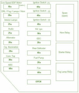
Fuse Box Ford 1996 Mustang Diagram

- 0 comments
Fuse Box Ford 1996 Mustang Diagram - Here are new post for Fuse Box Ford 1996 Mustang Diagram.

Fuse Box Ford 1996 Mustang Diagram


Fuse Box Ford 1996 Mustang Diagram

Fuse Panel Layout Diagram Parts: Turn Signal Lamps, Back-Up Lands, Rear Defroster, Top Relay Coil, Iluminated Entry Module, Hego (5.0), ABS, Low Oil Module, Low Coolant Module, Airbag Module, DRL Module, Safety Cluster Chime, Cluster Warning Lamps, O/D Module, Brake Shift Solenoid, Cluster Gauges, Shift Module, Generator Warning Light, Trunk Lamp, Low Beams, Door Locks,Fuel Pump, Cigar Lighter, EEC Power Relay Coil, Ignition Coil, TFI Module, Starter Relay, Clock Illumination, Speed Control Lamp, Radio, Power Windows, Head Lamps, Power Mirrors, Power Point, Power Seats.
[Continue reading...]

Paraphase Tone Controller

- 0 comments
As opposed to the widespread Baxandall circuit (dating back to 1952!) a ‘paraphrase’ tone control supplies a straight frequency response as long as the bass and treble controls are in the same position. This unique property makes the ‘paraphase’ configuration of interest if only treble or bass needs to be adjusted - it is not possible to adjust both at the same time! Essentially, it’s the difference in setting of the tone controls that determines the slope of the frequency response, and the degree of bass/treble correction. The circuit is simplicity itself, based on two networks C1-C2-C3/R9-R10-R11 and C5-C6-C7/R12-R13-R14.

Paraphase Tone Controller Circuit Picture:


The first is for the high frequencies (treble) response, the second, for the low frequencies (bass). The roll-off points have been selected, in combination with C4 and C8, for the sum of the two output signals to re-appear with a ‘straight’ frequency response again at the output. Roughly equal output levels from the networks are ensured by R6 = 7.15 k and R8 = 6.80 k. However, the operating principle requires the input signals to the two networks to be in anti-phase. For best operation the networks are driven by two buffers providing some extra gain.

Paraphase Tone Controller Circuit diagram:
  

The gain of IC1.D is slightly higher than that of IC1.C to ensure the overall response curve remains as flat as possible at equal settings of the tone controls. Because each network introduces a loss of about 1.72 (times), IC1.D and IC1.C first amplify the signal. The gain is set at about 8 (times) allowing input signal levels up to 1 V to pass the circuit at maximum gain and distortion-free. The gain also compensates the attenuation if you prefer to keep the tone controls at the mid positions for a straight response.

Parts and PCB layout:


Parts and PCB Layout
To audio fans, the circuit is rewarding to experiment with, especially in respect of the crossover point of the two networks. R3 and R4 determine the control range, which may be increased (within limits) by using lower resistor values here. The values shown ensure a tone control range of about 20 dB. IC1.B buffers the summed signal across R15. C9 removes any DC-offset voltage and R16 protects the output buffer from the effects of too high capacitive loads. R17, finally, keeps the output at 0 V. The choice of the quad opamp is relatively uncritical. Here the unassuming TL074 is used but you may even apply rail to rail opamps as long as they are stable at unity gain. Also, watch the supply voltage range. A simple circuit board was designed for the project. Linear-law potentiometers may be fitted directly onto the board. Two boards are required for a stereo application. The relevant connections on the boards are then wired to a stereo control potentiometer.

Specification:
  • Current consumption (no signal) 8 mA
  • Max. input signal 1 Veff (at max. gain)
  • Gain at 20 Hz +13.1 dB max. –6.9 dB min.
  • at 20 kHz +12.2 dB max. –7.6 dB min
  • Gain (controls at mid position) 2.38 x
  • Distortion (1 Veff, 1 kHz) 0.002% (B = 22kHz) 0.005% (B = 80 kHz)
COMPONENTS LIST
Resistors
R1-R4 = 10k
R5,R7 = 1k
R6 = 7k15
R8 = 6k80
R9,R10,R11 = 8k2
R12,R13,R14 = 2k2
R15 = 1M
R16 = 100R
R17 = 100k
P1,P2 = 100k preset or chassis-
mount control potentiometer, linear law
Capacitors
C1,C2,C3 = 47nF MKT, lead pitch 5mm
C4 = 68nF MKT, lead pitch 5mm
C5,C6,C7 = 10nF MKT, lead pitch 5mm
C8,C10,C11 = 100nF MKT, lead pitch 5mm
C9 = 2µF2 MKT, lead pitch 5mm or 7.5mm
Semiconductors
IC1 = TL074
Miscellaneous
K1,K2 = line socket, PCB mount, e.g.
T-709G (Monacor/Monarch)

Source:   http://www.ecircuitslab.com/2011/06/paraphase-tone-controller.html
[Continue reading...]

Speaker Headphone Switch Circuit Diagram For Computers

- 0 comments
If you need to use a headset with your PC, then you will know how frustrating it is continuously swapping over speaker and microphone cables. This is even worse if the PC is parked in a dark corner and the hard-to-read writing on the sound card sockets is covered in dust. This simple switch box eliminates all these problems. It sits on top of the desk and connects to the PC with stereo one-to-one cables.
On the rear of the box are sockets for the PC speaker and microphone connections and the existing speakers. On the front of the box are the sockets for the headset microphone and headphones, an input for an external microphone and two switches. One switch is used to direct the sound card output from the PC to either the existing speakers or the headphones.
Circuit diagram:
speaker-headphone-switch-circuit-diagram
Speaker-Headphone Switch Circuit Diagram
The second switch connects either the headset microphone or the external microphone to the input socket of the PC sound card. The switches used were 3 position 4 pole rotary switches with the last pole unused and adjusted for 2-position operation. All sockets were stereo 3.5mm types. This multiple switching arrangement is very flexible and is especially handy if you want to use an external microphone while monitoring with headphones. The ground wire as well as the left and right wires are all switched to prevent noise that could otherwise be induced into the microphone input through joining separate earths. For the same reason, a plastic case is used so that the earths of the sockets are not shorted together as would happen with a metal case. You will require two additional short stereo extension cables to connect the box to the PC.
Author: Leon Williams - Copyright: Silicon Chip Electronics
[Continue reading...]

TA7230P TA7236P TA7237AP amplifier schematic

- 0 comments
Amplifier circuit here is all based on the ic in the gains. Three IC TA7230P, TA7236P, TA7237AP is intregated circuit (IC) which was applied to the power amplifier. Each IC has a different output, different input voltage, all IC TA7230P, TA7236P, TA7237AP is manufactured by Toshiba.

You can see maximum minimum voltage , power output , and other here
TA7230P, TA7236P, TA7237AP amplifier schematic
[Continue reading...]

Making a Solar Energy Powered an iPhone Battery Charger

- 0 comments
The project was termed as Mighty Minty Boost as it was developed to function as iPod/iPhone charger with solar power. Aside from being small, it has a large battery capacity of 3.7V at 2000mAh and it accepts input power from 3.7V to 7V. As shown in the images below, it can become a compact USB power supply when the solar cell is removed after charging. The Velcro is used to secure the Mighty Minty Boost inside a backpack or messenger bag after unplugging the solar cell.

For faster charging, a larger solar cell can be attached to the bag. Enough power can be generated to fully charge an iPhone in about 5.5 hours and an iPod Touch in 4 hours using a slightly larger solar cell with 6V at 250mAh. The charger will automatically switch to trickle charging when the cell reaches full charge. The charging current is limited to 100mA when charging using the mini USB port and the charging is limited to 280mA when charging using the barrel plug jack

Hacks and Mods: iPhone Charger Powered Thru Solar Energy
.
The materials needed to build the charger include a small solar cell, Lithium Polymer battery charger, minty boost kit, adhesive backed Velcro, Altoids tin, connector/wire, and small double adhesive squares as shown in the images below. An input power that ranges from 3.7V to 7V maximum can be accepted by the single cell Lithium Polymer. In bright sunlight, the solar cell maxes out at approximately 5V at 100mA. A larger solar cell with 6V at 250mA can be used for faster charging.

Hacks and Mods: iPhone Charger Powered Thru Solar Energy

The images below show the assembly of minty boost kit where a JST connector is soldered to the minty boost PCB instead of connecting the battery holder in the kit. The minty boost circuit is allowed to connect to the Lithium Polymer battery charger circuit with this tiny connector. The minty boost is tested by connecting the battery pack and the charger circuit, the Lithium Polymer battery connects to the connector marked GND on the charger board and the minty boost connects to the connector marked SYS.

Hacks and Mods: iPhone Charger Powered Thru Solar Energy

To fit the charger, a notch is cut out of the other side of the Altoids tin and used double sided adhesive to secure the charging circuit to the bottom of the Altoids as shown below. The bottom of either one of the circuit boards should not touch the bottom of the Altoids tin while reconnecting the minty boost PCB and the battery to the charging circuit.

Hacks and Mods: iPhone Charger Powered Thru Solar Energy

Connecting or adding the solar cell can be done in different ways. Shortening the connector leads and plugging the barrel plug into the barrel jack on the charging circuit is one way. The other method is using another JST connector to replace the connector and plugging it into the third connector marked 5V on the charging circuit. Since there is no bog barrel plug sticking out of the side of the tin, using the second method is cleaner.

As shown in the photos below, some 2” Velcro was used to attach the solar cell to the top of the Altoids. To help protect the battery, a layer of clear packing tape was used for wrapping. N top of the two circuit boards, the battery pack is then set down. A red LED on the charger board will light up when the Mighty Minty Boost is set out in the bright sun. The iPod/iPhone/USB powered device can be connected once it is fully charged.

Hacks and Mods: iPhone Charger Powered Thru Solar Energy
[Continue reading...]

Jeep Cj2a Electrical Wiring Diagram Cable Harness Layout

- 0 comments
Electrical Wiring Diagrams on Wiring Diagram And Electrical Components Symbols For House Or Home
Wiring Diagram And Electrical Components Symbols For House Or Home.


Electrical Wiring Diagrams on Wiring Diagram   Automotive Wiring Diagrams And Electrical Diagrams
Wiring Diagram Automotive Wiring Diagrams And Electrical Diagrams.


Electrical Wiring Diagrams on The Jeep Cj2a Electrical Wiring Diagram And Cable Harness Layout
The Jeep Cj2a Electrical Wiring Diagram And Cable Harness Layout.


Electrical Wiring Diagrams on Small Engine Magnetos   Lawn Mower Snow Blowers Atv Bicycle Engine
Small Engine Magnetos Lawn Mower Snow Blowers Atv Bicycle Engine.


Electrical Wiring Diagrams on Chevy S 10 Blazer Ignition Control  Ic  Circuit Wiring Diagram
Chevy S 10 Blazer Ignition Control Ic Circuit Wiring Diagram.


Electrical Wiring Diagrams on Gfci Outlet Wiring Diagram   Pdf  55kb
Gfci Outlet Wiring Diagram Pdf 55kb.


Electrical Wiring Diagrams on Typical Electric Water Heater Construction   Wiring Diagram
Typical Electric Water Heater Construction Wiring Diagram.


Electrical Wiring Diagrams on Light Switch Diagram  Power Into Light     Pdf  44kb
Light Switch Diagram Power Into Light Pdf 44kb.


Electrical Wiring Diagrams on Vulcan Vn750 Electrical System And Wiring Diagram   Circuit Schematic
Vulcan Vn750 Electrical System And Wiring Diagram Circuit Schematic.


Electrical Wiring Diagrams on Way Switch Wiring Diagram Variation  6   Electrical Online
Way Switch Wiring Diagram Variation 6 Electrical Online.


[Continue reading...]

Video Amplifier

- 0 comments
The video amplifier in the diagram is a well-known design. Simple, yet very useful, were it not for the ease with which the transistors can be damaged if the potentiometers (black level and signal amplitude) are in their extreme position. Fortunately, this can be obviated by the addition of two resistors. If in the diagram R3 and R4 were direct connections, as in the original design, and P1 were fully clockwise and P2 fully anticlockwise, such a large base current would flow through T1 that this transistor would give up the ghost.

Video Amplifier Circuit diagram:


Moreover, with the wiper of P2 at earth level, the base current of T2 would be dangerously high. Resistors R3 and R4 are sufficient protection against such mishaps, since they limit the base currents to a level of not more than 5 mA. Shunt capacitor C4 prevents R4 having an adverse effect on the amplification.

Author: L.A.M. Prins - Copyright: Elektor Electronics

Source :  http://www.ecircuitslab.com/2011/06/video-amplifier-circuit-diagram.html
[Continue reading...]

1975 Cadillac DeVille Wiring Diagrams

- 0 comments
1975 Cadillac DeVille Wiring Diagrams
(click for full size image)

The Part of  1975 Cadillac DeVille Wiring Diagrams: dual beam, starter motor, electric choke, oil pressure switchhigh beam, light switch, gas gauge tank unit, license light, cruise control wiring,brake switch, right hand marker lamp, hazard flasher, turn flasher, headlight dimmer switch, trunk light & switchprinted circuit connector, 
[Continue reading...]

Wednesday, April 10, 2013

SP LED light weight Box

- 0 comments
For beginners, its their 1st project that offers them a lift. And so as to induce that, its continuously necessary to create positive that the project that you just choose is basically helpful. One such project is that the RGB light-weight fader. this is often quite straightforward and may be done simply by a beginner. scan on to understand a lot of concerning this.


 Concerning twenty LEDs are needed here. begin by wiring all the LEDs and connecting it to a breadboard. this is often quite a tedious method and takes quite plenty of your time.

 ensuing step is to create the ability board. Quite plenty needs to be done to drive all the LEDs employing a single PWM channel. therefore to atone for this, a multiplexer IC is employed. a couple of voltage conversions is also needed in such a case.


 As mentioned earlier, one PWM is employed to regulate 3 totally different channels. The MSP430 is employed to modify between the various channels. this offers the impression that there are 3 individual channels. There is also some problems with the glint, however this might not be a show stopper downside.

 The supply code for running the circuit is kind of sophisticated . concerning twelve totally different modes are gift here and switching between the assorted modes is finished employing a single push button.
 
 
http://streampowers.blogspot.com/2012/07/sp-led-light-weight-box.html 
[Continue reading...]

Network Lead Tester Circuit

- 0 comments

This is a circuit for confirming the continuity and correct wiring of computer network leads which have 8 wires, but it can be used to check any lead with up to 8 wires by using appropriate connectors. For example stereo audio leads with 5-pin DIN plugs can be checked by just using the first 5 LEDs. The tester is simple but it can save a great deal of time when making up leads and it is much cheaper than the more sophisticated alternatives. This is the figure of the circuit;


The tester works by connecting each wire to an output at one end and an LED at the other end. The outputs are switched on one at a time in sequence so that a correctly wired lead will make each LED light in turn. The 4017 IC counts up to 10 so there is a pause (for the 9th and 10th counts) before the LED sequence repeats. If the LEDs light up in the wrong sequence one (or both) of the connectors is wired wrongly. If an LED fails to light it indicates a broken connection. Please note that the RJ45 computer network plugs cannot normally be re-wired, instead they must be cut off and replaced.
[Continue reading...]

Simple Pseudo Random Glitter

- 0 comments
A question recently asked on the Elektor website forum was how to make several white LEDs ‘sparkle’. The helpful author has not only provided a useful suggestion (use a random effect), but also devel-oped a suitable circuit and even designed a PCB layout. You can download the Eagle files for this from the Elektor website page for this article (www.elektor.com, archive # 080329-1.zip).

But first let ’s consider the basic question: artificial sparkling or glittering can best be simulated by having the different light sources switch on randomly at a par ticu-lar frequency. Surprisingly enough, it is not all that easy to generate truly random se quencesele ctronically. However, the electronic ran-domness does not necessarily have to be perfect for glitter applications. Patterns that appear to be random are suf-ficient for the desired visual impression.
LED Circuit Diagram

Based on this principle, the author uses two 556 timer ICs to generate signals whose frequencies (850 Hz for IC1a and 180 Hz for IC1b) can be divided by each other with-out yielding an integer divisor. A decimal counter oper-ated in an unconventional manner uses these two signals to produce a constantly pseudo-random pattern on its ten outputs, which repeats itself only very infrequently. This behaviour is obtained by applying the higher frequency signal to the CLK input of counter IC2, with the CLK Inhibit input on pin 13 being driven by the lower-frequency signal. The result is ‘genuine pseudo-random’ blinking.

LEDs can be connected directly to the ten outputs, since a CMOS output can anyhow only supply a few milli ampères. However, it is recommended to use series resistors (2.2 kΩ to 4.7 kΩ) to reduce the load on the IC out-puts if the supply voltage is higher than 10 V. If you want to have more than ten LEDs glitter, you can naturally build several copies of this circuit. Link
Author : Hans-Jürgen Zons - Copyright : Elektor
[Continue reading...]

LM3914 battery level indicator

- 0 comments
LM3914 battery level indicator
Battery level indicator circuit is a circuit that is used to measure the battery voltage / battery. The main components of the battery level indicator circuit is an LM3914 IC. LM 3914 on Circuit battery level indicator is a monolithic IC that detects an analog voltage. And drive the 10 LEDs that produce a linear analog display on a given input voltage.

IC LM3914 is easy to get in the market and not expensive. IC LM3914 battery level indicator on the circuit is often encountered in a series of peak indicator audio signals in analog audio equipment. Battery level indicator circuit consists of IC LM3914, 10 pieces of LED, and a few resistors. The scheme of  battery level indicator can be seen below.

LM3914 battery level indicator

In the circuit of the battery level indicator on the supply circuit voltage taken from the battery / batteries through a switch. Didesaimn this circuit will only display the battery level when the switch is pressed. This is intended to save the battery voltage itself.
[Continue reading...]
 
Copyright © 2012. Fast Diagrams - Posts · Comments
Powered by Blogger