Showing posts with label a. Show all posts

Thursday, October 16, 2014

12V to 120V DC DC Converter Circuit

- 0 comments

12V to 120V DC DC Converter Circuit

Here is a simple DC DC converter schematic using a saturation-limited to push-pull converter. DC converter can be used to power the VCR from a car battery and glow plug light aircraft models from a 12V battery starter.

As a final amplifier of the DC DC converter is a pair of transistor MJE2955 and 2SC945 as oscillator to apply sufficient bias to the final amplifier transistors.

The 2SC945 is a bias switch for startup. When applying 12V power, this transistor applies enough bias to the power transistors to get the oscillation started. Soon later, the 100uF capacitor charges up, the transistor goes off, and the power transistors self-bias into cut-off, such that cross-conduction is eliminated. After removing power, the 6k8 resistor discharges the bias timing capacitor, as otherwise the circuit would be unable to restart!

The secondary rectifiers are ultrafast diodes. These are NOT 1N4007! And the 220nF capacitors for the secondary filter are no typos; the diodes deliver almost pure DC, since the oscillation waveform is square, so only some noise filtering is needed. No electrolytics are necessary here.

12V

DC DC Converter

Note the filters at both input and output, using ferrite cores. These are necessary to avoid polluting your environment with RF noise! Using these filters, and joining the input and output negative leads, this converter is very quiet and does not cause any problem in my combined HF, VHF and UHF station.

All ferrite cores (for the transformer and for the noise filters) are manufactured by Amidon Associates, and can be ordered directly from them in small quantities. Look for Amidon on the web. The 77-material core used for the transformer is less than ideal. A square-loop ferrite would work more efficiently! This one gets really warm, operating in saturation mode at 25 kHz. But it has worked well enough for two years now. The filter cores, on the other hand, are well chosen, so try to use the exact ones.

For all windings, the schematic states the number of turns. “7t” means 7 turns. As the transformer is quite small for the involved power, use as thick a wire as you can fit, leaving about half of the space for the 2×7 turns primary winding, and the other half for the secondary, while the feedback winding can be made from very thin wire.

The transistors do not need any heat sinks. They are large enough without, and they need to dissipate little heat!

[Continue reading...]

Wednesday, October 15, 2014

Build a Fly back Transformer Driver Circuit Diagram

- 0 comments
This is an efficient flyback driver for modern cylindrical rectified television flybacks. Many sites doesnt provide circuits driving these transformers, they simply say that they are bad.

I dont agree. In fact I built this circuit. I spent a lot of time for finding resonant frequency (around 15Khz) and duty cycle. These transformers best work at around 90% duty cycle. You may notice corona breakdown at terminals and pfffff sound (as well as the ozone smell) when adjusting the off time trimmer to near 500-300 ohms. Of course it will work for other tipes of flyback as frequency and duty cycle have a large range.

 Flyback Transformer Driver Circuit Diagram


Flyback


Frequency range can be increased using multiposition switch for other values of C3 capacitor ,for example 2 nF for 80KHz-200000KHz, but didnt found flybacks with so high resonant frequencies, in addition with higher values of c3 , eg 200nF, 2uF the
frequency will drop making possible the use of ignition coils, and rectified power transformers @50Hz to charge high voltage electrolitic caps at 300-400V). Unfortunately my ignition coil died because insulation breakdown (too long drawn arcs)...
I was able to power a small (20cm) Spark Gap tesla coil Using these dc rectified flybacks to charge primary tank capacitor.
The operation is simple
The 555 is wired as an astable and the capacitor is charged only through the 4,7Kohm trimmer (notice the diode) and discharged only through the 2.2 Kohm trimmer, making the duty cycle full adjustable. The square wave is then feed in a totem pole made up of a 2N3904 and a 2N3906, which are cheap, and easy to find. The totem pole ensures the gate being charged and discharged very fast (approx 50nS i think). The IRF840 is a cheap (i found it for 4euros) reliable and powerful power mosfet, it has current capability of 8 A continuous and 32A pulse, 800V drain source voltage, protecting internal zener diode. There is a snubbing network to ensure that voltage spikes are kept low (unless the insulation of the transformer start to leak) protecting both transistors and 555 IC. 100 ohm is a compromise between decay time and voltage spike.
Comments and specifications:
The 100 ohm snubber must me a 5W resistor, or it will burn at long operations
The led is only for safety purposes
Use a dead man switch (pushbutton) for safety
The power supply must supply at least 2-3 A if you want decent arcs (20000 KV)
Dangers:
The flyback driven in this way can supply a significant current, aldough the heart fibrillation starts at 30mA
I recommend caution to avoid painful arc-burns.
The arc is a hot plasma, never operate the circuit in presence of flammable substances.
Charging high voltage capacitors is a serious life threat, so if you arent unexperienced just draw arcs and no more

This device when rectified generates static voltage that can be a little annoying.... (or fun, i sprayed with corona a plastic pen from positive terminal and then i was able to attract little pieces of paper)
Disclaimer:
I dont assume any responsibility of the damages or discruptions dove by this device, to persons or things. Any irresponsable action would be a serios danger. This is high voltage threat it with respect.

author: Jonathan Filippi
[Continue reading...]

Friday, October 3, 2014

5 Watt Class A Audio Amplifier

- 0 comments

On the day of the old valve, most commercial audio amplifiers suitable for compact integrated single discs or players used stereo amplifier topology of a single valve. The circuit is usually carried out through a multiple type valve, for example, a triode pentode ECL86.

Common features of the amplifiers are Class A operation, the output power in the 3 - 5W range, input sensitivity of about 600mV of total output power, THD of 3% @ 1KHz and 3W. Best types showed figures of 1.8% THD @ 3W and 0.8% @ 2W.

This solid-state push-pull single-ended Class A circuit is capable of providing a sound comparable to that of tube amplifiers, offering more output power (6.9W measured across a load of 8 ohm speaker cabinet), less THD, higher input sensitivity and better linearity.

Voltage and current for this circuit is 24 V and 700 mA, respectively, compared with 250 HT rail and 1A@6.3V heating filament of the valve works with amplifiers. The penalty only for the transistor circuit that works with the need for a larger heat sink for Q2 and Q3 (compared with the maximum power delivered). In any case, the amount of heat generated by this circuit can be comparable to that of a single valve amplifier. A choice of low-boost facility can be added through R5 and C5.

This circuit was built and compared with a circuit of a valve box phonograph in the early 1950 by Aren van Waard, a Dutch biochemist working in the field of medical imaging (PET) with a strong interest in audio amplifiers valve. A complete description of the circuits and test results of subjective comparisons made by the distinguished author appeared in the magazine AudioXpress: February, March and April 2005 issues.
[Continue reading...]

Monday, September 1, 2014

A Low Cost Hearing Aid

- 0 comments

This low-cost, general-purpose electronic hearing aid works off 3V DC (2x1.5V battery). The schema can be easily assembled on a veroboard. For easy assembling and maintenance, use an 8-pin DIP IC socket for TDA2822M.


In this schema, transistor Q1 and associated components form the audio signal preamplifier for the acoustic signals picked up by the condenser microphone and converted into corresponding electrical signals. Resistor R5 and capacitor C3 decouple the power supply of the preamplifier stage. Resistor R1 biases the internal schema of the low-voltage condenser microphone for proper working. The audio output from the preamplifier stage is fed to the input of the medium-power amplifier schema via capacitor C2 and volume control P1.
The medium-power amplifier section is wired around popular audio amplifier IC TDA2822M (not TDA2822). This IC, specially designed for portable low-power applications, is readily available in 8-pin mini DIP package. Here the IC is wired in bridge configuration to drive the 32-ohm general-purpose monophonic earphone. Red LED (D1) indicates the power status. Resistor R8 limits the operating current of D1. The audio output of this schema is 10 to 15mW and the quiescent current drain is below 1 mA.


Parts:

P1 = 10K
R1 = 2.2K
R2 = 330K
R3 = 680R
R4 = 33R
R5 = 100R
R6 = 4.7R
R7 = 4.7R
R8 = 220R
C1 = 0.01uF-10V
C2 = 100nF-63V
C3 = 47uF-10V
C4 = 10uF-10V
C5 = 0.01uF-10V
C6 = 100uF-10V
C7 = 100nF-63V
C8 = 100nF-63V
D1 = Red LED
Q1 = BC547
IC1 = TDA2822M
EP1 = Mono Earphone 32R
SW1 = On-Off Switch

[Continue reading...]

Friday, December 27, 2013

Build a Thermo Fan To Keep Your Amp Cool Circuit Diagram

- 0 comments
How to Build a Thermo-Fan To Keep Your Amp Cool Circuit Diagram


 Thermo-Fan To Keep Your Amp Cool Circuit Diagram

Build a Thermo-Fan To Keep Your Amp Cool Circuit Diagram

[Continue reading...]

Build a 60Hz Power Inverter Circuit Diagram

- 0 comments
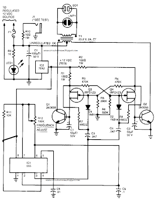
Hi Friends to we build a simple 60Hz Power Inverter Circuit Diagram.In the 60Hz Power Inverter Circuit Diagram Capacitor C5 and potentiometer R12 determine the frequency of the output signal at pin 3 of IC1, the 555 oscillator. The output signal is differentiated by C3 and C4 before it`s input to the base of power transistors Q1 and Q2 via diodes D1 and D2, respectively. 

The signal from !C1 is adjusted to 120Hz, because the flip-flop formed by transistors Q3 and Q4.divides the frequency by 2.When Q3 is on, the base of Q1 is connected via R1 to the regulated 12-V supply. Then, when the flipflop changes states, Q4 is turned on and the base of Q2 connected to the 12-V supply through R2. The 100 mA base current allowsQ1 and Q2 to alternately conduct through their respective halves to the transformer`s secondary winding. 

 60Hz Power Inverter Circuit Diagram

60Hz Power Inverter Circuit Diagram


To eliminate switching transients caused by the rapid switching of Q3 and Q4, capacitors C1 and C2 filter the inputs to the base of Q1 and Q2 respectively. Power for the unit comes from an automobile`s 12V system or from a storage battery. The power is regulated by IC2, a 7812 regulator. LED1, connected across the 12-V input, can be used to indicate whether power is being fed to the circuit. The neon pilot lamp, LMP1, shows a presence or absence of output power.


[Continue reading...]

Sunday, December 22, 2013

Build a Stand by Power Circuit Diagram for Non Volatile Cmos Rams

- 0 comments
This is  a simple Stand by Power Circuit diagram for Non Volatile Cmos Rams. To prevent loss of data when a CMOS RAM is switched from normal operation (Vcc = 5 volts) to stand-by mode (Vcc = VBAT) it must be ensured that the CS pin goes near the Vcc rail at all times. 

Ac coupling to the chip select is made through capacitor C, breaking the dc current path between Vqq (and hence VBAT) and the decoder output. So, whatever the impedance state of the decoder in power down, the battery will provide current only for the RAM, low enough to keep the voltage at CS near to V^.

Power Circuit Diagram

Build a Stand by Power Circuit Diagram for Non Volatile Cmos Rams Circuit diagram

[Continue reading...]

Tuesday, May 28, 2013

How to make a simple motor

- 0 comments
This is a simple moter circuit.These pictures show how to make a simple motor.first of all you should take two plates that I have mentioned bellow.and set it up on a wooden plate as picture 3 has shown.Then after take coils and wrap it around the plastic stick. When the stick rotates the coil should have a contact with the current supplier so after wrapping place the coil as picture shows.place a magnet middle of the stick as picture shows.


[Continue reading...]

Thursday, April 11, 2013

Making a Solar Energy Powered an iPhone Battery Charger

- 0 comments
The project was termed as Mighty Minty Boost as it was developed to function as iPod/iPhone charger with solar power. Aside from being small, it has a large battery capacity of 3.7V at 2000mAh and it accepts input power from 3.7V to 7V. As shown in the images below, it can become a compact USB power supply when the solar cell is removed after charging. The Velcro is used to secure the Mighty Minty Boost inside a backpack or messenger bag after unplugging the solar cell.

For faster charging, a larger solar cell can be attached to the bag. Enough power can be generated to fully charge an iPhone in about 5.5 hours and an iPod Touch in 4 hours using a slightly larger solar cell with 6V at 250mAh. The charger will automatically switch to trickle charging when the cell reaches full charge. The charging current is limited to 100mA when charging using the mini USB port and the charging is limited to 280mA when charging using the barrel plug jack

Hacks and Mods: iPhone Charger Powered Thru Solar Energy
.
The materials needed to build the charger include a small solar cell, Lithium Polymer battery charger, minty boost kit, adhesive backed Velcro, Altoids tin, connector/wire, and small double adhesive squares as shown in the images below. An input power that ranges from 3.7V to 7V maximum can be accepted by the single cell Lithium Polymer. In bright sunlight, the solar cell maxes out at approximately 5V at 100mA. A larger solar cell with 6V at 250mA can be used for faster charging.

Hacks and Mods: iPhone Charger Powered Thru Solar Energy

The images below show the assembly of minty boost kit where a JST connector is soldered to the minty boost PCB instead of connecting the battery holder in the kit. The minty boost circuit is allowed to connect to the Lithium Polymer battery charger circuit with this tiny connector. The minty boost is tested by connecting the battery pack and the charger circuit, the Lithium Polymer battery connects to the connector marked GND on the charger board and the minty boost connects to the connector marked SYS.

Hacks and Mods: iPhone Charger Powered Thru Solar Energy

To fit the charger, a notch is cut out of the other side of the Altoids tin and used double sided adhesive to secure the charging circuit to the bottom of the Altoids as shown below. The bottom of either one of the circuit boards should not touch the bottom of the Altoids tin while reconnecting the minty boost PCB and the battery to the charging circuit.

Hacks and Mods: iPhone Charger Powered Thru Solar Energy

Connecting or adding the solar cell can be done in different ways. Shortening the connector leads and plugging the barrel plug into the barrel jack on the charging circuit is one way. The other method is using another JST connector to replace the connector and plugging it into the third connector marked 5V on the charging circuit. Since there is no bog barrel plug sticking out of the side of the tin, using the second method is cleaner.

As shown in the photos below, some 2” Velcro was used to attach the solar cell to the top of the Altoids. To help protect the battery, a layer of clear packing tape was used for wrapping. N top of the two circuit boards, the battery pack is then set down. A red LED on the charger board will light up when the Mighty Minty Boost is set out in the bright sun. The iPod/iPhone/USB powered device can be connected once it is fully charged.

Hacks and Mods: iPhone Charger Powered Thru Solar Energy
[Continue reading...]

Monday, April 8, 2013

Short Circuit Protection With A MOSFET

- 0 comments
If you have an application in which a MOSFET is already used to switch a load, it is relatively easy to add short-circuit or overload protection. Here we make use of the internal resistance RDS(ON), which produces a voltage drop that depends on the amount of current flowing through the MOSFET. The voltage across the internal resistance can be sensed using simple comparator or even a transistor, which switches on at a voltage of around 0.5V. You can thus avoid the use of a sense resistor (shunt), which usually produces an undesirable extra voltage drop. The comparator can be monitored by a microcontroller. In case of an overload, the software can initiate suitable countermeasures (PWM regulation, alarm, emergency stop etc.). It is also conceivable to connect the comparator output directly to the gate of the MOSFET, in order to immediately cut off the transistor in case of a short circuit.

Short-Circuit Protection With A MOSFET Circuit Diagram
[Continue reading...]

Saturday, April 6, 2013

A Dice Circuit Using LED

- 0 comments
This is a design circuit for a game a dice. This circuit uses 7 LED to simulate the rolling of a dice after the Roll button is pushed. It has a slowdown feature so that you can see the rolling of the dice slowing down and then stop. This is more satisfying than the usual LED dice circuit which just stops after the button is released. This circuit is work with based on 555 IC and 14017. IC 14017 is decade counter. This is the circuit figure.


The principle work of the circuit is when the switch is turned on Q4 is turned off (its base is pulled high by the 3.3M ohm resistor) and the 555 oscillator is not oscillating. Pressing the ROLL switch immediately charges the 470nF capacitor, Q4 is turned ON and the 555 starts to oscillate. The 470nF gradually discharges via the 10M ohm and 3.3M ohm resistors and turns Q4 off. The 555 is connected as an oscillator. The frequency of oscillation is generally independent of the potential difference across the pins. However, as Q4 turns off the frequency becomes dependent on the voltage. The counter CP0 is advanced by a LOW to HIGH transition from pin 3 of the 555 to pin 14. The first six outputs from the 14017 labeled are labeled by O0 to O5. The next output O6 from pin 5 is connected to the Reset pin 15.


[Continue reading...]
 
Copyright © 2012. Fast Diagrams - Posts · Comments
Powered by Blogger